
In-situ fabrication method for silicon solar cell

a solar cell and fabrication method technology, applied in the field of in-situ fabrication methods of solar cells, can solve the problems of inability to replace traditional energy, high cost of the above method for solar cells, and complicated solar cell fabrication art, etc., and achieve the effect of reducing the production cost of solar cells and greatly reducing the fabrication of solar cells

Inactive Publication Date: 2014-10-28
INST OF MICROELECTRONICS CHINESE ACAD OF SCI
View PDF5 Cites 0 Cited by
  • Summary
  • Abstract
  • Description
  • Claims
  • Application Information

AI Technical Summary

Benefits of technology

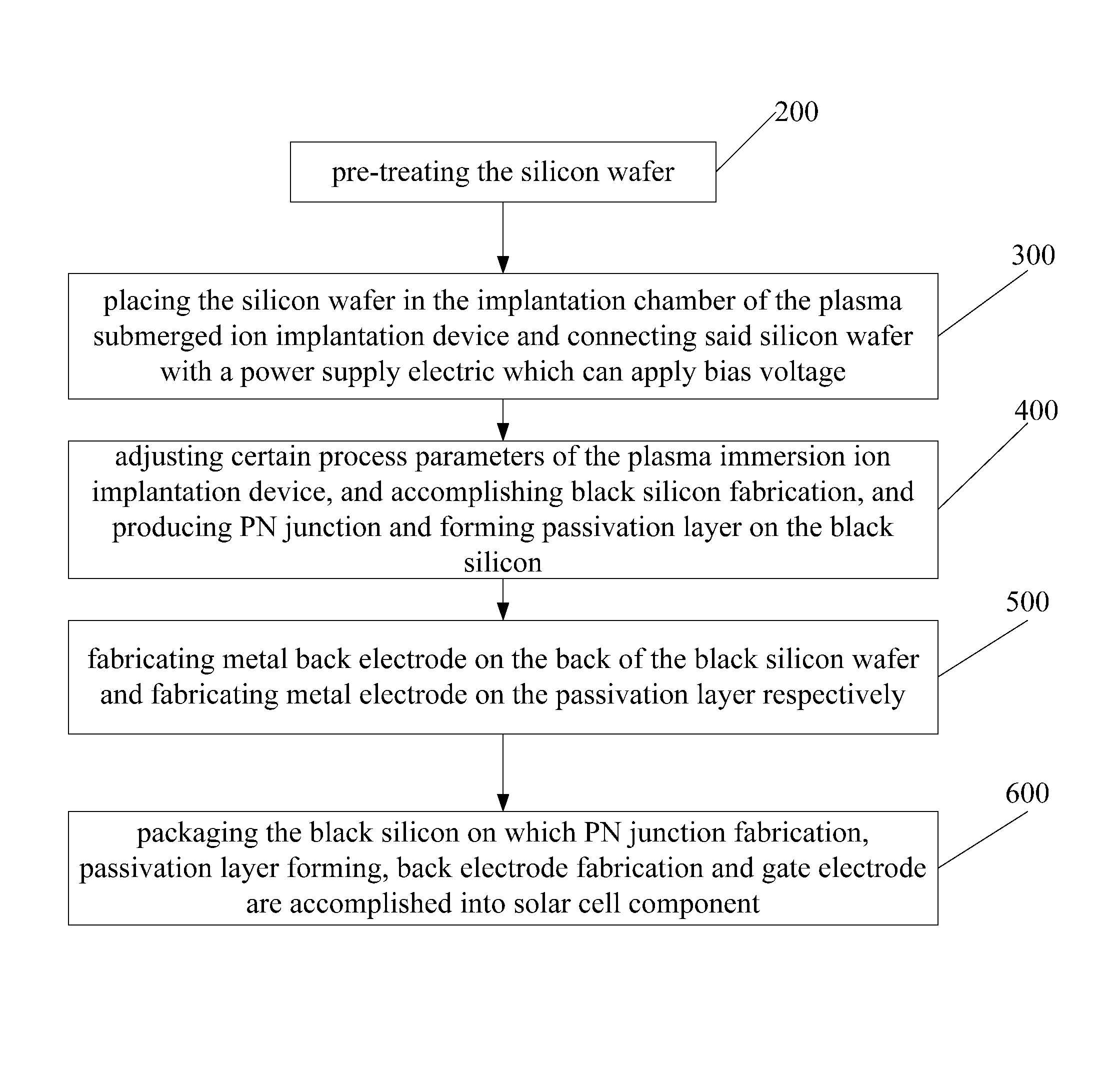
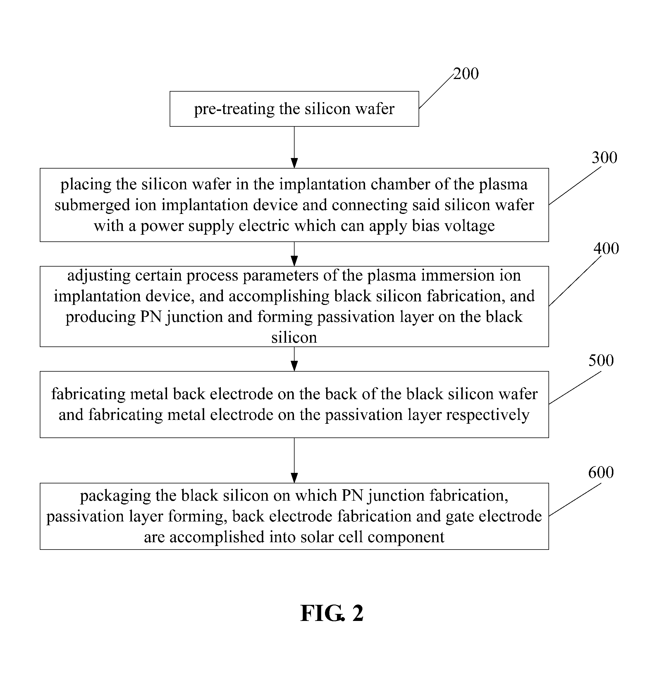
The present invention provides an in-situ fabrication method for solar cell that can achieve black silicon fabrication, PN junction production, and passivation layer forming in a single process. This method reduces the devices needed for solar cell fabrication, decreases production costs, and simplifies the process control. Additionally, doping chalcogenide elements can expand the absorption spectrum of black silicon and increase the infrared absorption rate, leading to higher photoelectric convention efficiency of solar cells.

Problems solved by technology

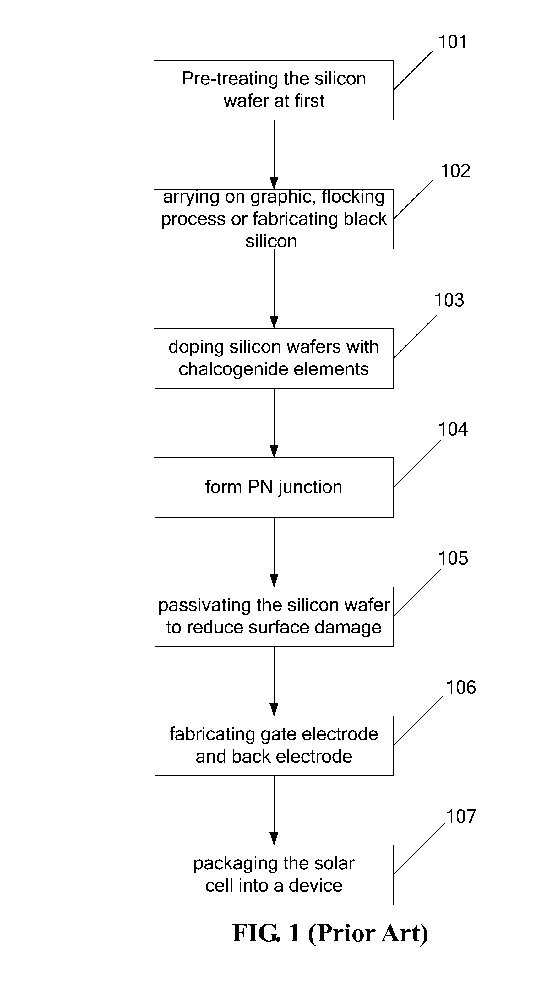
In the fabrication method of solar cell above, procedures corresponding to step 101 to 107 need to be achieved in different devices, which make fabricating art of the solar cell be complicated and the controllability or art be worse.
More importantly, the cost of the above method for solar cell is too high, therefore it cannot replace traditional energy, and large scale of solar application is limited.

Method used


Image

  • In-situ fabrication method for silicon solar cell
  • In-situ fabrication method for silicon solar cell
  • In-situ fabrication method for silicon solar cell

Examples


Embodiment Construction

[0034]To further comprehend the following detailed description of the present invention, reference is made to the attached drawings and embodiments.

[0035]Plasma Immersion Ion Implantation (PIII in short), is also called plasma implantation, plasma doping, plasma immersion implantation, plasma source ion implantation, plasma base ion implantation and etc. The several names mean the same process technology, that is, sample to be implanted is immersed into plasma, and by applying bias voltage (also called “implantation voltage”) to the sample, implantation sheath layer is formed between the sample and the plasma; reactive ions located on the implantation sheath layer electric field and reactive ions entering sheath layer electric field from the plasma are implanted into the sample under the speeding effect of electric field. Sheath layer is formed on the sample surface, so the sample surface exposed to the plasma will be implanted throughout.

[0036]In the present invention, plasma immer...


PUM

PropertyMeasurementUnit
bias voltageaaaaaaaaaa
volume ratioaaaaaaaaaa
temperatureaaaaaaaaaa

Abstract

An in-situ fabrication method for a silicon solar cell includes the following steps: pretreating a silicon chip; placing the pretreated silicon chip in an implantation chamber of a plasma immersion ion implantation machine; completing the preparation of black silicon via a plasma immersion ion implantation process; making a PN junction and forming a passivation layer on the black silicon; after making the PN junction and forming the passivation layer, removing the black silicon from the plasma immersion ion implantation machine; preparing a metal back electrode on the back of the black silicon; preparing a metal grid on the passivation layer; obtaining a solar cell after encapsulation. Said method enables black silicon preparation, PN junction preparation, and passivation layer formation in-situ, greatly reducing the amount of equipment needed for the preparation of solar cells and the preparation cost. In addition, the method is simple and easy to control.

Description

CROSS REFERENCE TO RELATED APPLICATIONS[0001]The present application is a 35 U.S.C. §371 National Phase conversion of International (PCT) Patent Application No. PCT / CN2010 / 076716, filed on Sep. 8, 2010, the disclosure of which is incorporated by reference herein. The PCT International Patent Application was published in Chinese.TECHNICAL FIELD[0002]The present invention relates to the field of solar cell device fabrication technology, particularly to an in-situ fabrication method for silicon solar cell.BACKGROUND OF THE INVENTION[0003]Facing to the environmental problems such as greenhouse effect, acid rain and other ones caused by current energy crisis and mass cost of chemic fuel, it is urgent to develop and utilize new energy efficiently worldwide. Solar energy is a kind of reproducible energy which is easily obtained and green. It will become the main body of the worldwide energy supply before long. Solar cell, regarded as clean and efficient green continuable energy, will provi...

Claims


Application Information

Patent Timeline
Patent Type & Authority Patents(United States)
IPC IPC(8): C23C14/48H01L21/223H01L31/18H01L21/26
CPCH01L21/2236Y02E10/547C23C14/48H01L31/1804H01L31/18Y02P70/50
Inventor XIA, YANGLIU, BANGWULI, CHAOBOLIU, JIEWANG, MINGGANGLI, YONGTAO
Owner INST OF MICROELECTRONICS CHINESE ACAD OF SCI
Learn More