Atomic force microscopy active optical probe

an active optical probe and atomic force technology, applied in scanning probe microscopy, instruments, measurement devices, etc., can solve the problems of inability to achieve high-cost optical resolution and light power, inability to achieve high-power optical output, etc., to achieve high performance, wide gain spectrum, and low cost

Active Publication Date: 2016-11-01
ACTOPROBE LLC
View PDF1 Cites 16 Cited by
  • Summary
  • Abstract
  • Description
  • Claims
  • Application Information

AI Technical Summary

Benefits of technology

[0013]In addition to unique imaging and spectroscopy capabilities, the AAOP technology provides an exciting opportunity for obtaining both space- and time-resolved optical/chemical information. Currently, a variety of techniques are used to measure ultrafast dynamics of surface adsorbates [Liang 1994, Frontiera 2011, Laaser 2013]. These methods, however, are limited in their spatial resolution to the far-field diffraction limit. TERS has the potential to overcome this limitation, but integration of external pulsed excitation source with TERS for time-resolved spectroscopy is very challenging [Klingsporn 2014, Pozzi 2014, Wickramasinghe 2014]. In contrast, the AAOP technology naturally provides the ultrafast time-resolved spectroscopy capability. The monolithically integrated semiconductor laser sources with specialized gain media with very broad gain spectrum, such as InAs quantum dots, offer mode-locking capabilities for sub-picosecond pulse generation [Huang 2001, Rafailov 2007]. The integration of ultrafast pulsed laser source into GaAs AFM probe will allow probing the nonlinear response of chemical systems and provide site-specific information about the molecular dynamics.
[0014]Practice of the present invention can be advantageous to provide high performance, low cost probes for atomic force microscopy with enhanced functionality to include that of NSOM, TERS, or hybrid AFM. The AAOP with its integrated light source and detector has the potential to outperform the above-mentioned technologies for optical characterization at the nanoscale.
[0015]The high refractive index of GaAs accounts for a resolution increase compared to hybrid AFM that employs an optical microscope in the far field: the resolution increases by the factor of the refractive index of GaAs (˜3.6). Since light source and detector are integrated into the probe, the difficulty of focusing the optical microscope on the correct surface area does not apply. This also puts the detector very close to the sample, which results in increased sensit...

Problems solved by technology

This high-cost approach suffers from inherent limitations in terms of optical resolution and light power that can be delivered.
To achieve high lateral resolution the size of the near-field aperture needs be reduced, thus leading to an exponential decrease of optical power output.
This approach has limited applications to near-field microscopy with ultimate resolution of about 50 nm, but is not appropriate for optical spectroscopy because of small power output.
The hybrid approach has only been shown to work in research labs and it is difficult to imagine how optical probes can be fabricated cost-effecti...

Method used


Image

  • Atomic force microscopy active optical probe
  • Atomic force microscopy active optical probe
  • Atomic force microscopy active optical probe

Examples


embodiment 1

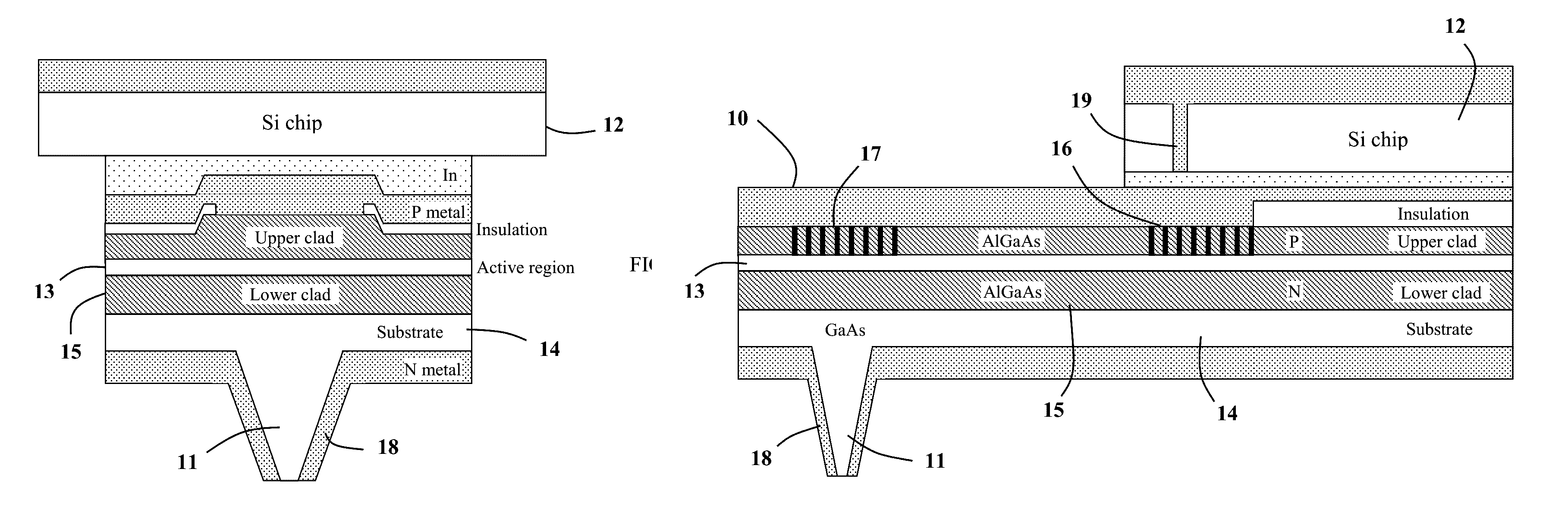
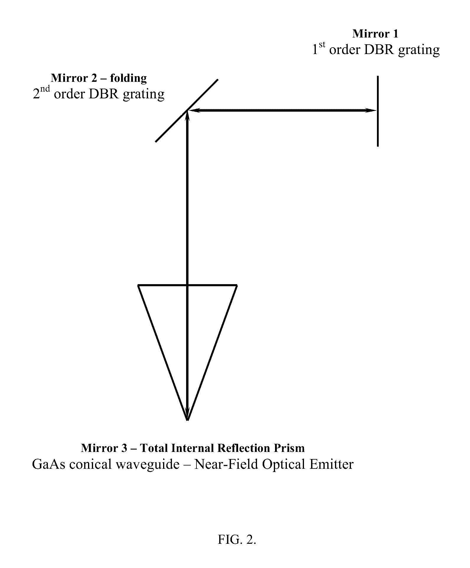
[0030]The envisioned AFM Active Optical Probe (AAOP) is shown in FIGS. 1A, 1B, and 1C. In FIG. 1A, we present a cross-sectional view of the probe. In FIG. 1B, a side view is shown, and in FIG. 1C a bottom view is shown. The AAOP consists of a cantilever 10 with the AFM probe tip 11 mounted on a conventional Si chip 12 (3.4 mm×1.6 mm×0.3 mm). The AAOP is designed as an intra-cavity probe, i.e. the AFM probe is part of the laser cavity as shown in an equivalent optical schematic of the device in FIG. 2. This increases laser light coupling into the optical near field at the apex of the AFM probe by a factor of 10,000 [Partovi 1999]. The AAOP is a very efficient optical near-field nano-emitter.

[0031]The most widely used probes for atomic force microscopy are fabricated using silicon technology. In contrast, the AAOPs are fabricated from GaAs, a semiconductor material suitable as the basis for optical device fabrication. The laser and detector functionality is enabled by an epitaxially g...

embodiment 2

[0040]In another embodiment of the present invention the mirrors #1 and #2 of the laser cavity can be in the form of facets obtained by cleaving or etching the laser wafer or by applying Focused Ion Beam (FIB) in proper directions (FIG. 6). For example, mirror #1 22 can be fabricated by cleaving or etching the wafer perpendicular to the epitaxial layers. Mirror #2 (the folding mirror) 23 can be fabricated using FIB applied in such a way as to create a flat surface at 45° with respect to the wafer surface.

embodiment 3

[0041]In yet another embodiment of the present invention, the laser 15 is a second-order distributed feedback (DFB) surface-emitting laser that employs its second-order waveguide grating 24 to outcouple the laser light vertically into the AFM tip 11 fabricated from the laser substrate 14 (FIG. 7).

[0042]Again, the light generated by the laser is coupled into the surface mode of the GaAs probe tip (conic shape micro-prism) and transferred to the tip apex. Practice of the present invention can be easily extended to graded second-order DFB lasers for much more efficient power extraction in order to increase the optical power delivered to the GaAs probe tip. Graded second-order DFB lasers employ aperiodic gratings with symmetrically changing grating period to achieve a very significant enhancement of power extraction in vertical direction [Xu 2012].


PUM


Abstract

A new active optical Atomic Force Microscopy (AFM) probe integrating monolithically a semiconductor laser source, an AFM tip, and a photodetector into a robust, easy-to use single semiconductor chip to enable both conventional AFM measurements and optical imaging and spectroscopy at the nanoscale.

Description

CROSS REFERENCE TO RELATED APPLICATIONS[0001]This application claims benefit and priority of U.S. provisional application Ser. No. 62 / 282,529 filed Aug. 4, 2015, the entire disclosure of which is incorporated herein by reference.FIELD OF THE INVENTION[0002]The present invention relates to AFM microscopy and near-field optical microscopy probes and, in particular, to an integrated AFM active optical probe capable of performing both conventional AFM measurements and optical imaging and spectroscopy at the nanoscale.BACKGROUND OF THE INVENTION[0003]Optical characterization at the nanoscale currently requires instruments such as NSOM (near-field scanning optical microscope), TERS (tip-enhanced Raman spectroscopy), or hybrid AFM (that includes a specialized far-field optical microscope).[0004]Attempts at integrating atomic force microscopy and optical techniques have already been made and several products based on these schemes have found their way into the market. Commercially available...

Claims


Application Information

Patent Timeline
IPC IPC(8): G01Q60/22
CPCG01Q60/22G01Q20/04G01Q60/06G01Q70/14
Inventor UKHANOV, ALEXANDER A.SMOLYAKOV, GENNADY A.
Owner ACTOPROBE LLC
Why Eureka
Try Eureka