
Electromagnetic wave absorbing sheet and method of manufacturing the same and electronic device using the same

a technology of electromagnetic wave and absorbing sheet, which is applied in the direction of shielding materials, transportation and packaging, synthetic resin layered products, etc., can solve the problems of generating inductive noise, electromagnetic wave interference problems affecting other devices, emi (electromagnetic interference), etc., and achieves excellent electromagnetic wave absorbing rate, high productivity, and simple manufacturing process

Active Publication Date: 2017-11-28
AMOSENSE
View PDF47 Cites 10 Cited by
  • Summary
  • Abstract
  • Description
  • Claims
  • Application Information

AI Technical Summary

Benefits of technology

The present invention provides an electromagnetic wave absorbing sheet which has high imaginary part permeability in a frequency band of 300 MHz or higher. The sheet is made by separating an amorphous alloy ribbon into multiple pieces using flake-processing. The sheet can absorb electromagnetic waves from electronic components and prevent them from interfering with other components. The sheet is thin and can be easily manufactured, making it highly productive and cost-effective. The sheet has increased demagnetizing field to reduce hysteresis loss, improved permeability uniformity, and minimized heat generation.

Problems solved by technology

Such components accompany a rapid change of the voltage and current by a high-speed signal, to thus generate inductive noise as a source of generating high frequency noise.
These components such as active components and passive components are located very close together on a printed circuit having printed wires, to thereby cause cross-talk problems caused by electromagnetic coupling between internal components or between the components and the wires in small digital electronic devices, or radiate electromagnetic waves out of the small digital electronic devices to thereby cause EMI (ElectroMagnetic Interference: EMI) or electromagnetic wave interference problems which affect the other devices.
In addition, electromagnetic waves generated from electronic devices which are long-term exposed to the human body, may affect the human body, to thus cause diseases such as glaucoma, and reduction of fertility.
The electromagnetic shielding which is proposed as measures against EMI problems means that the electromagnetic noise generated from the inside of the electronic device is not radiated to the outside of the case, and also electromagnetic noise entering from the outside is absorbed or blocked.
However, since electronic components are mounted at a high density on printed circuit board (PCB) in the case of small digital electronic devices, the above-described measures against noise are not suitable as urgent measures against noise for products of a short product life.
This is because mounting spaces are insufficient for mounting filters in the small digital electronic devices, and miniaturization and thinning should be taken in a design stage.
The current magnetic material has a problem that it does not meet the thinning and the conductive noise suppression effect, in a lower frequency band or a higher frequency band than about 10˜100 MHz.
The Korean Patent No. 10-0755775 has a limit to reduce the thickness since a plate-like carbon powder that is a resistance body powder and a plate-like Sendust® powder that is a soft-magnetic material powder are oriented in an insulating polymer matrix, and has low imaginary part permeability because of the relatively low permeability when compared with those of different types of magnetic sheets, to thereby increase a sheet price because of the use of an expensive soft magnetic powder of a low absorbing rate.
In addition, in the case of a polymer magnetic sheet containing the soft-magnetic powder, and in the case of increasing the thickness of the sheet to improve the low magnetic permeability, the material cost is further increased with an increase in the thickness, and it is difficult to cope with the thinning tendency of mobile terminals.
Furthermore, the noise suppressing film is commercially available as a thick film of 0.2 mm or above and thus has a limit in use.
However, the sheet proposed in Korean Patent Laid-open Publication No. 10-2005-37015 is a kind of the polymer sheet, and has a low permeability problem.
However, the electromagnetic wave shielding material manufactured according to the Korean Patent Laid-open Publication No. 10-2003-86122 shield electromagnetic waves in a way of reflecting most of the electromagnetic waves by the metal foil ribbon and the metal film coated or vacuum deposited on the metal foil ribbon, but does not shield electromagnetic waves in a manner that absorbs the electromagnetic waves.
However, the above Korean Patent Laid-open Publication No. 10-2009-123776 shields electromagnetic waves in a way of reflecting most of the electromagnetic waves by the nickel and copper plating layers, but does not shield electromagnetic waves in a manner that absorbs the electromagnetic waves.
As a result, when the conductive foam sheet is used in the inside of the electronic device, adjacent other circuit elements are affected by the electromagnetic wave reflected from the conductive foam sheet.
However, in the same manner as that of the Korean Patent Laid-open Publication No. 10-2009-123776, the electromagnetic wave shielding sheet disclosed in the Korean Patent Laid-open Publication No. 10-2009-78620 may cause a problem of affecting adjacent other circuit elements due to the electromagnetic wave reflected from the metal deposition layer.
As a result, in general, the mobile terminals seeking lightweight, thinning, shortening, and compactness may not use the shielding sheet when the thickness of the shielding sheet exceeds 0.5 mm.
Further, when depositing a conductive metal layer on a surface of the synthetic resin film, electromagnetic wave shielding performance may be reduced since the peeling of the conductive metal layer may occur.

Method used


Image

  • Electromagnetic wave absorbing sheet and method of manufacturing the same and electronic device using the same
  • Electromagnetic wave absorbing sheet and method of manufacturing the same and electronic device using the same
  • Electromagnetic wave absorbing sheet and method of manufacturing the same and electronic device using the same

Examples


examples 8 to 11

[0127]Final samples (ARS2-454, ARS2-456, ARS2-457, and ARS2-459) of 40 μm thick of Examples 8 to 11 were prepared by comprising: making an amorphous ribbon made of a Fe67B14Si1Co18 alloy in a thickness of 25 μm by a rapid solidification method (RSP) due to melt spinning; cutting the amorphous ribbon in a sheet form and heat treating the cut sheet at 454° C., 456° C., 457° C., and 459° C., respectively, under no magnetic field, in a nitrogen (N2) atmosphere, for 1 hour, to thereby prepare a laminate sheet of 45 μm thick in the same manner as the Example 1; and performing flake-processing and laminate-processing respectively.

[0128]Permeability values according to the frequency changes were obtained with the samples of Examples 8 to 10, which were illustrated in graphs of FIGS. 13A to 13C.

[0129]In addition, power loss values were measured by using a micro-strip line method shown in FIG. 16, with the samples of Examples 8 to 11, which were illustrated in a graph of FIG. 14.

[0130]The sam...


PUM

PropertyMeasurementUnit
sizeaaaaaaaaaa
thicknessaaaaaaaaaa
frequencyaaaaaaaaaa

Abstract

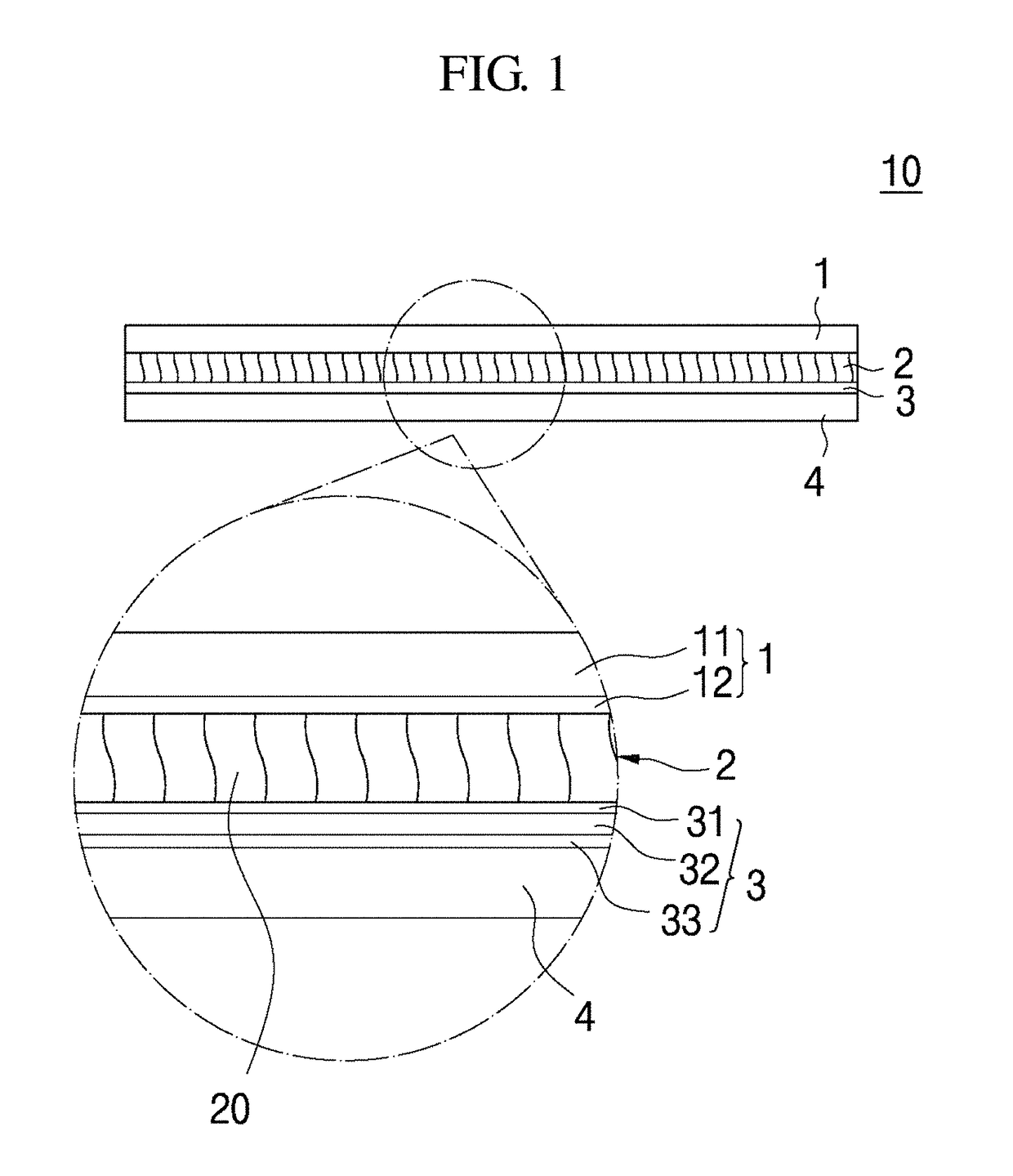
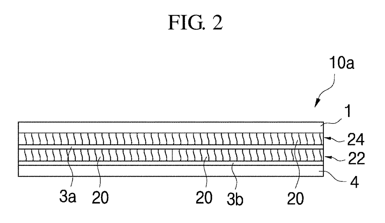
Provided are an electromagnetic wave absorbing sheet which is a thin film and a low cost and has an excellent electromagnetic wave absorbing rate, a method of manufacturing the same, and an electronic device using the same. The electromagnetic wave absorbing sheet includes: at least one layer thin-film magnetic sheet which is separated into a plurality of fine pieces; a protective film that is adhered on one surface of the thin-film magnetic sheet; and a double-sided tape that is adhered on the other surface of the thin-film magnetic sheet.

Description

TECHNICAL FIELD[0001]The present invention relates to an electromagnetic wave absorbing sheet and a method of manufacturing the same, and more particularly to an electromagnetic wave absorbing sheet which is thin and inexpensive, and has an excellent electromagnetic wave absorbing rate, a method of manufacturing the same, and an electronic device including the electromagnetic wave absorbing sheet.BACKGROUND ART[0002]In recent years, demand for high-speed signal processing, high function, miniaturization of a product, and reducing the thickness of a product shape in an electronic device circuit in association with digital electronic equipment, has been being accelerated. Data processing speeds of various types of semiconductor devices mounted on a printed circuit board (PCB) become high, and thus the component mounting density of active components and passive components mounted on the printed circuit board (PCB) is also going high.[0003]Such components accompany a rapid change of the...

Claims


Application Information

Patent Timeline
Patent Type & Authority Patents(United States)
IPC IPC(8): H01F1/34B32B7/12H01Q17/00H01F1/16H05K9/00H01Q1/52B32B15/04
CPCH05K9/0075B32B15/04H01F1/16H01Q1/52H01Q17/00H05K9/0081B32B7/12Y10T428/32B32B2307/208B32B2307/702B32B2307/704H01F1/34Y10T156/10Y10T428/25Y10T428/26Y10T428/2804Y10T428/2848B32B27/08H05K9/00
Inventor JANG, KIL JAELEE, DONG HOONKIM, KI CHUL
Owner AMOSENSE
Learn More