
Mask blank, phase shift mask, and production method thereof

a mask and mask technology, applied in the field of mask blanks and phase shift masks, can solve problems such as difficulty in processing fine patterns, affecting the processing efficiency of masks, and affecting the processing efficiency of masks, and achieves the effect of favorable pattern processing, high light shielding properties, and low emf bias

Active Publication Date: 2018-05-15
DAI NIPPON PRINTING CO LTD
View PDF8 Cites 1 Cited by
  • Summary
  • Abstract
  • Description
  • Claims
  • Application Information

AI Technical Summary

Benefits of technology

This configuration provides high light-shielding properties while reducing EMF bias, enabling the production of phase shift masks with improved pattern processability and resistance suitable for lithography techniques on wafers with half pitches from 40 nm and beyond.

Problems solved by technology

Here, a transmittance of the half-transparent pattern film is conventionally designed to be approximately 6%, but the problem is that a transferred image becomes unclear due to the exposure light transmitted to this half-transparent pattern film, in the place where an area of the mask pattern portion is large.
However, if the light-shielding pattern film is thickened, a resist pattern for processing the light-shielding pattern film is also required to be thickened, which makes the processing of a fine pattern difficult.
Also, a malfunction such as a pattern collapse during washing may be caused since the heights of the light-shielding pattern film and half-transparent pattern film are increased in the step of processing a mask.
Also, with regard to a binary mask to be used for a half-pitch (hp) of a pattern on a wafer from 40 nm on, the width of a mask pattern line on a photomask becomes smaller than the wavelength 193 nm of ArF excimer laser exposure light to be used for a lithography; a problem is that a value of bias (EMF bias) which is a correcting amount of a mask line width derived from the effect of an electro magnetics field (EMF) increases when the film thickness of a light-shielding pattern film in a mask pattern region is thick, since an oblique light incidence lighting method and a super resolution technique using a pupil filter have been adopted in order to form a fine pattern.
Then, such a problem arises also in a half tone type phase shift mask (try tone mask) having the above described light shielding pattern film.

Method used


Image

  • Mask blank, phase shift mask, and production method thereof
  • Mask blank, phase shift mask, and production method thereof
  • Mask blank, phase shift mask, and production method thereof

Examples


first embodiment

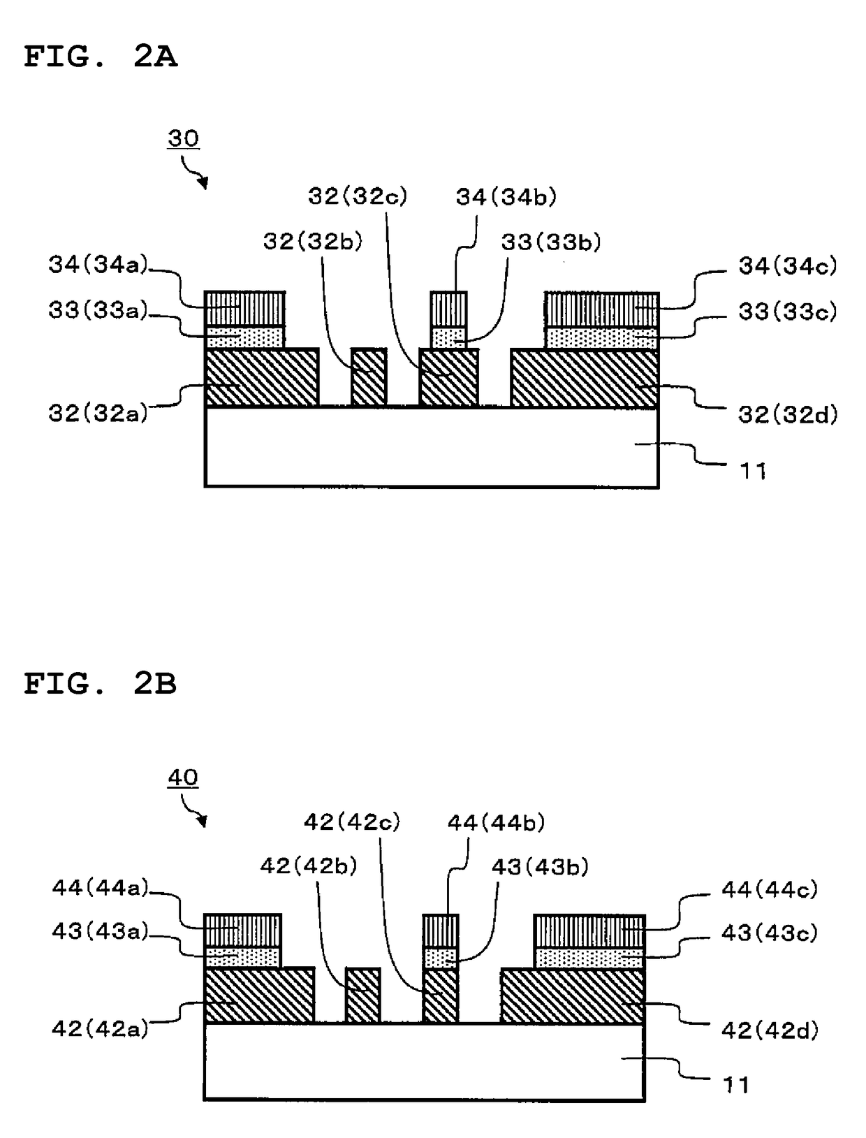
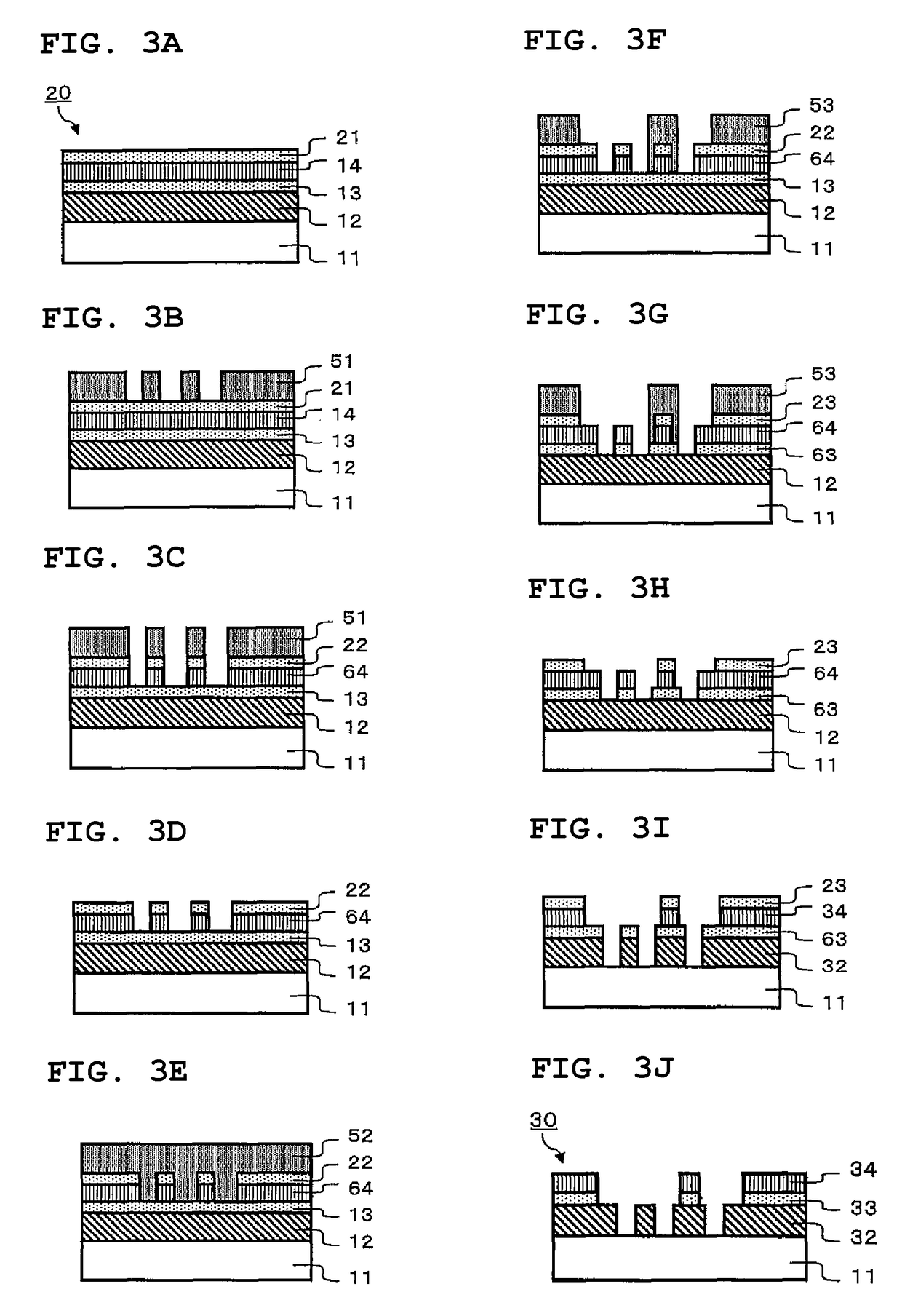
[0115]FIGS. 3A to 3J are schematic sectional views illustrating an example of a producing method for a phase shift mask 30 in a form shown in FIG. 2A.

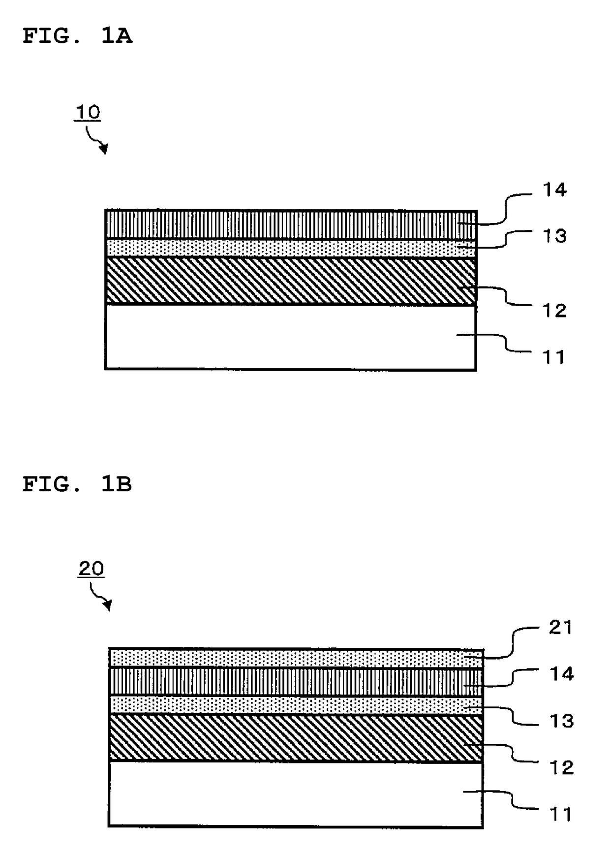
[0116]In order to obtain the phase shift mask 30 by the producing method of the present embodiment, for example, as shown in FIG. 3A, prepared is a mask blank 20 with a hard mask layer, in which a hard mask layer 21 is formed on a light shielding layer 14 of a mask blank 10 having a transparent substrate 11, a half-transparent layer 12 formed on the transparent substrate 11, a middle layer 13 formed on the half-transparent layer, and a light-shielding layer 14 formed on the middle layer 13.

[0117]Next, formed on the hard mask layer 21 is a first resist pattern film 51, by a resist plate making using electron beam lithography, for example (FIG. 3B).

[0118]Next, a first form of a hard mask pattern 22 is formed by etching the hard mask layer 21 exposed from the first resist pattern film 51 by dry etching using chlorine-based gas for example...

second embodiment

[0123]FIGS. 4A to 4J are schematic sectional views illustrating an example of a producing method for a phase shift mask 40 in a form shown in FIG. 2B.

[0124]In order to obtain the phase shift mask 40 by the producing method of the present embodiment, for example, first, as shown in FIG. 4A, prepared is a mask blank 20 with a hard mask layer, in which a hard mask layer 21 is formed on a light-shielding layer 14 of a mask blank 10 having a transparent substrate 11, a half-transparent layer 12 formed on the transparent substrate 11, a middle layer 13 formed on the half-transparent layer, and a light-shielding layer 14 formed on the middle layer.

[0125]Next, a first resist pattern film 54 is formed on the hard mask layer 21 by means of a resist making plate using electron beam lithography, for example (FIG. 4B).

[0126]Next, the hard mask layer 21 exposed from the first resist pattern film 54 is etched by dry etching using chlorine-based gas, for example, so as to form a first form of a har...

example 1-1

[0132]Prepared was a mask blank 20 with a hard mask layer by using: an optically polished 6 inch square and 0.25 inch thick synthetic quartz as a transparent substrate 11; a molybdenum silicide oxide film (MoSiO) as a half-transparent layer 12; a 3 nm film-thick chromium film (Cr) as a middle layer 13; a silicon film (Si) as a light-shielding layer 14; and a 2 nm chromium film (Cr) as a hard mask layer 21.

[0133]Here, the film thickness of the half-transparent layer 12 was adjusted so that the transmittance with respect to the exposure light became 6%; and the film thickness of the light-shielding layer 14 was adjusted so that the optical density of a laminated body, in which three kinds of layers: the half-transparent layer, the middle layer, and the light-shielding layer are laminated, with respect to the light exposure became 3.0.

[0134]The optical density was measured by MCPD3000 manufactured by OTSUKA ELECTRONICS Co., LTD; an optical constant may be obtained by an ellipsometer (m...


PUM

PropertyMeasurementUnit
thicknessaaaaaaaaaa
optical densityaaaaaaaaaa
refractive indexaaaaaaaaaa

Abstract

The present invention provides a mask blank including: a transparent substrate, a half-transparent layer for controlling a phase and a transmittance of the exposure light, formed on the transparent substrate, a middle layer formed on the half-transparent layer, and a light-shielding layer formed on the middle layer, wherein the light-shielding layer is constituted with a single metal material not including a transition metal; a film thickness of the light-shielding layer is 40 nm or less; and an optical density of a laminated body, in which three kinds of layers: the half-transparent layer, the middle layer, and the light-shielding layer are laminated, with respect to the exposure light is a value to the extent that the laminated body functions as a light-shielding region or more; the mask blank is used for producing a half tone type phase shift mask, and suitable for a lithography technique on a wafer from 40 nm half pitch and on for its high light-shielding property even thinning the light-shielding pattern film, capability of decreasing the value of EMF bias, and excellency in pattern processability, light-shielding property and chemical resistance.

Description

TECHNICAL FIELD[0001]The present invention relates to a mask blank to be used for producing a semiconductor element, a phase shift mask and a producing method for the phase shift mask; in specific, relates to a half tone type phase shift mask to be used for a lithography technique, of which a half-pitch of a pattern on a wafer is from 40 nm on, when transferring a mask pattern on the wafer by using a high NA light exposing apparatus.BACKGROUND ART[0002]High integration and refinement of a semiconductor element has been improved from a design rule 45 nm node to 32 nm node; further, the development of a semiconductor element with the node of 22 nm or less has been in progress. In order to achieve these high integration and refinement of a semiconductor element, presently used technique is a photolithography technique for transferring a pattern on a wafer by using a photo mask by means of an optical projection exposing apparatus utilizing an ArF excimer laser with the light exposure wa...

Claims


Application Information

Patent Timeline
Patent Type & Authority Patents(United States)
IPC IPC(8): G03F1/32G03F1/54
CPCG03F1/54G03F1/32
Inventor WATANABE, HIROSHIHAYANO, KATSUYATAKAMIZAWA, HIDEYOSHIOHKAWA, YOUHEIADACHI, TAKASHITANI, AYAKOMIURA, YOICHI
Owner DAI NIPPON PRINTING CO LTD
Learn More