Multilayer printed wiring board and its manufacturing method, and resin composition for filling through-hole

Inactive Publication Date: 2009-10-27
IBIDEN CO LTD
View PDF73 Cites 19 Cited by
  • Summary
  • Abstract
  • Description
  • Claims
  • Application Information

AI Technical Summary

Benefits of technology

[0022]The present invention solves the aforementioned problems inherent in the conventional techniques, and the present inven

Problems solved by technology

These through-holes are, however, considered as dead spaces in designing of a circuit, and hence become one of the factors which prevent wiring from densifying.
In addition, since coefficients of thermal expansion between the resin and a metal are different, the conductor layer on the through-holes may peel or form cracks due to heat cycle.
In a printed wiring board as is described in Japanese Unexamined Patent Publication No. 4-92496, gaps or voids tend to form because of poor adhesion between the conductor layer and the electric conductive material in the through-holes.
The formation of voids between the electric conductive material and a through-hole causes delamination of the conductor layer or generation of cracks on the through-hole in the use at high temperature and high humidity conditions due to air or water accumulated in the voids.
The pad is, however

Method used


Image

  • Multilayer printed wiring board and its manufacturing method, and resin composition for filling through-hole
  • Multilayer printed wiring board and its manufacturing method, and resin composition for filling through-hole
  • Multilayer printed wiring board and its manufacturing method, and resin composition for filling through-hole

Examples


example 1

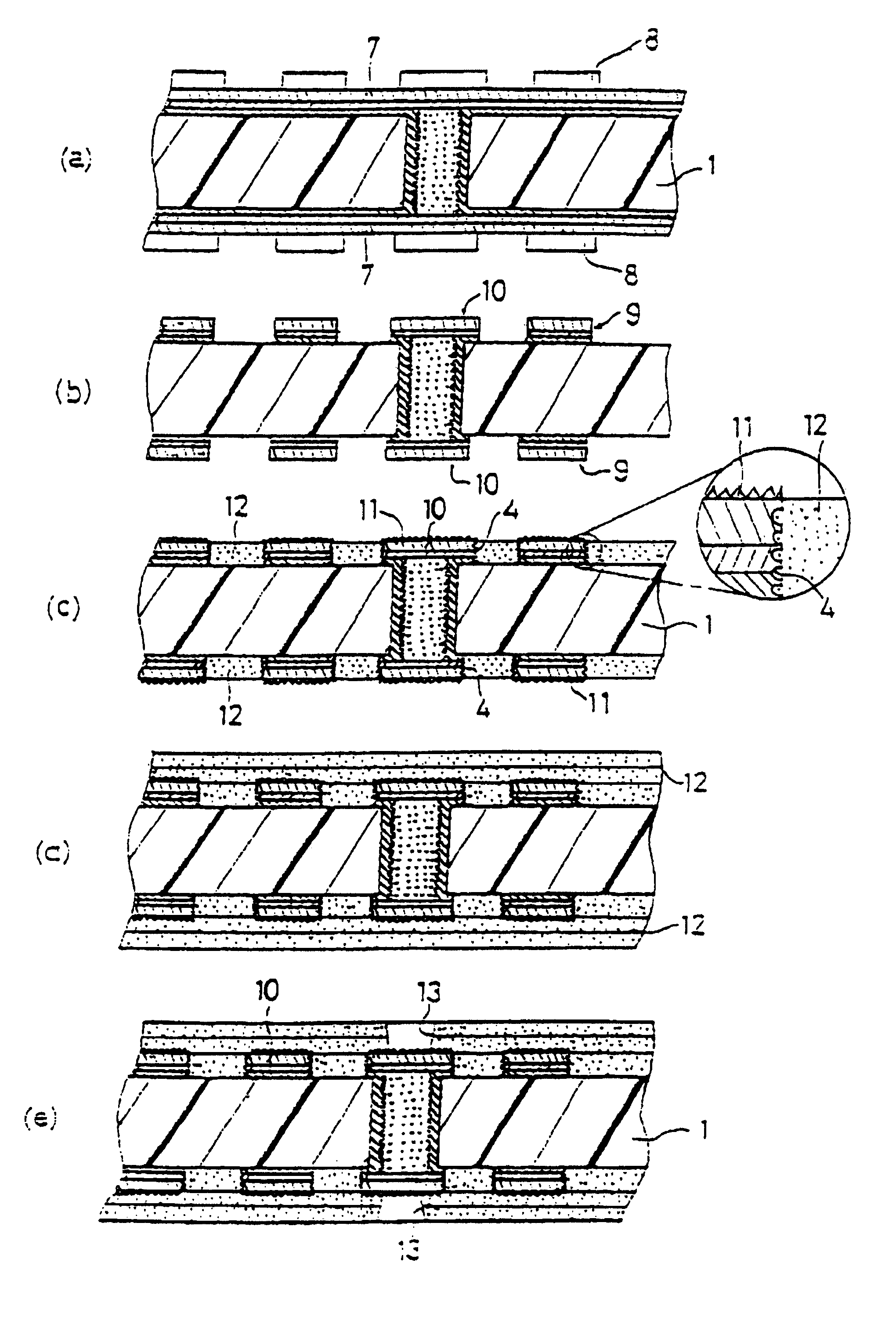
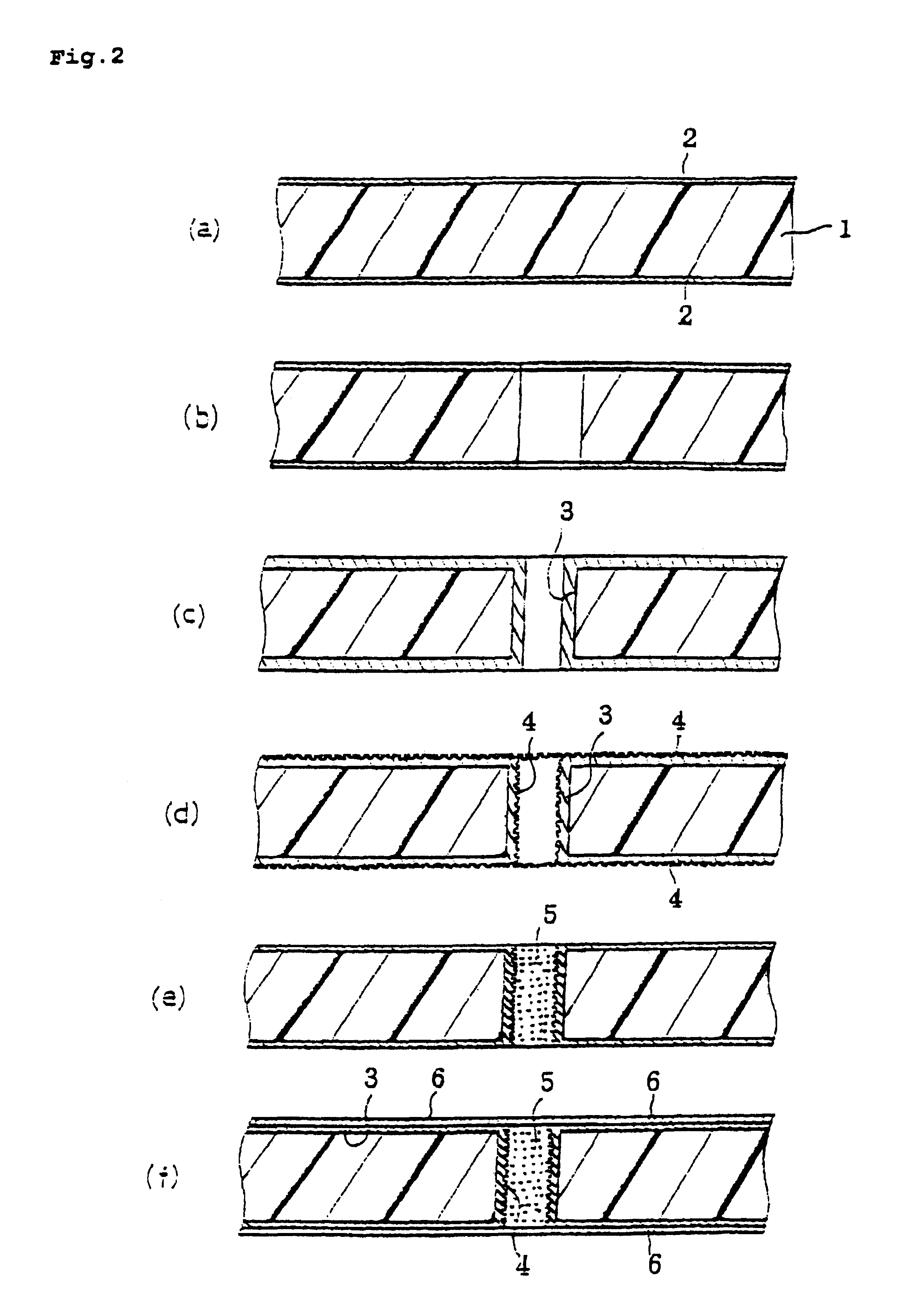
[0153](1) As a starting material, was employed a copper-clad laminate (manufactured by Matsushita Electric Works, Ltd., trade name: R4737) composed of a substrate 1 of a polytetrafluoroethylene resin (hereinafter briefly referred to as trade name: Teflon) of 0.8 mm in thickness and a copper foil 2 of 18 μm in thickness laminated on the substrate 1, the surface adjacent to the copper foil 2 being roughened (see FIG. 2(a)). Initially, the copper-clad laminate was drilled to form a hole and the internal surface of the hole was treated with a modifier (manufactured by Junkosha Co., Ltd., trade name: Tetraetch) composed of an organic metallic sodium to improve the wettability of the surface (see FIG. 2(b)).

[0154]A palladium-tin colloid was then applied to substrate, and the substrate was immersed in an electroless plating solution having the following composition to form an electroless plated film of 2 μm in thickness all over the surface of the substrate.

[0155]

EDTA150g / lCopper sulfate20...

example 2

Multilayer Core Substrate

[0173](1) A two-sided copper-clad laminate 1′ of 0.5 mm in thickness was prepared, and provided with an etching resist on both surfaces, and subjected to an etching treatment with an aqueous solution of sulfuric acid and hydrogen peroxide to obtain a substrate provided with conductor circuits. A glass-epoxy prepreg and a copper foil 2 were in turn laminated onto both surfaces of the substrate, pressed at a temperature raging from 165 to 170° C. and a pressure of 20 kg / cm2 to give a multilayer core substrate 1′ (see FIG. 5(a)).[0174](2) The multilayer core substrate 1′ was then drilled to form through holes having a diameter of 300 μm (see FIG. 5(b)), applied with a palladium-tin colloid and then immersed in an electroless plating solution having the same composition as in Example 1 to form an electroless plated film of 2 μm in thickness all over the substrate. The substrate was then subjected to an electrolytic copper plating in the same condition as in Exam...

example 3

[0198]A multilayer printed wiring board was manufactured in the same manner as in Example 1, except that when through-holes were filled with a copper paste, a through-hole-covering conductor layer 10 for covering an exposed copper paste from the through-holes was not formed. According to this process, pits might be formed because the surface of the copper paste was frequently removed in the formation of openings on an insulating resin layer by a laser beam irradiation.


PUM

PropertyMeasurementUnit
Lengthaaaaaaaaaa
Lengthaaaaaaaaaa
Thicknessaaaaaaaaaa

Abstract

A multilayer printed wiring board is composed of a substrate provided with through-holes, and a wiring board formed on the substrate through the interposition of an interlaminar insulating resin layer, the through-holes having a roughened internal surface and being filled with a filler, an exposed part of the filler in the through-holes being covered with a through-hole-covering conductor layer, and a viahole formed just thereabove being connected to the through-hole-covering conductor layer. Without peeling between the through-holes and the filler, this wiring board has a satisfactory connection reliability between the through-holes and the internal layer circuit and provides a high density wiring.

Description

BACKGROUND OF THE INVENTION[0001]1. Field of the Invention[0002]This invention relates to a multilayer printed wiring board used as a package board for mounting an IC chip or the like and a process of producing the same, and more particularly to a multilayer printed wiring board capable of providing a high density wiring easily and of preventing the formation of cracks or the like in through-holes or in the neighborhood thereof when heat cycle occurs, for example.[0003]This invention also relates to a resist composition for filling through-hole of a multilayer printed wiring board, which composition is used for ensuring satisfactory electric connections between viaholes and through-holes even at high temperature and high humidity conditions or under such conditions as to cause heat cycle.[0004]2. Discussion of Background Information[0005]In general, through-holes are formed for electrically connecting the front surface to the back surface of a core substrate (hereinafter referred to...

Claims


Application Information

Patent Timeline
IPC IPC(8): B32B3/00H05K3/00H05K3/38H05K3/46
CPCH05K3/0094H05K3/4602Y10T428/24917H05K3/384H05K3/385H05K3/4069H05K2201/0209H05K2201/0212H05K2201/0215H05K2201/0257H05K2201/0347H05K2201/09536H05K2201/09563H05K2201/0959H05K2201/096Y10S428/901H05K3/383B32B3/00
Inventor ASAI, MOTOOSHIMADA, KENICHINODA, KOUTAKARIYA, TAKASHISEGAWA, HIROSHI
Owner IBIDEN CO LTD
Why Eureka
Try Eureka