
Hybrid nanostructured materials based in II-VI semiconductors

a technology of nanostructured materials and semiconductors, applied in the field of organic-organic-organic hybrid composites, can solve the problems of restricting use and several limitations in the ability to change optical properties, and achieve significant quantum confinement effects and advantages for device making

Inactive Publication Date: 2010-07-13
RUTGERS THE STATE UNIV
View PDF7 Cites 2 Cited by
  • Summary
  • Abstract
  • Description
  • Claims
  • Application Information

AI Technical Summary

Benefits of technology

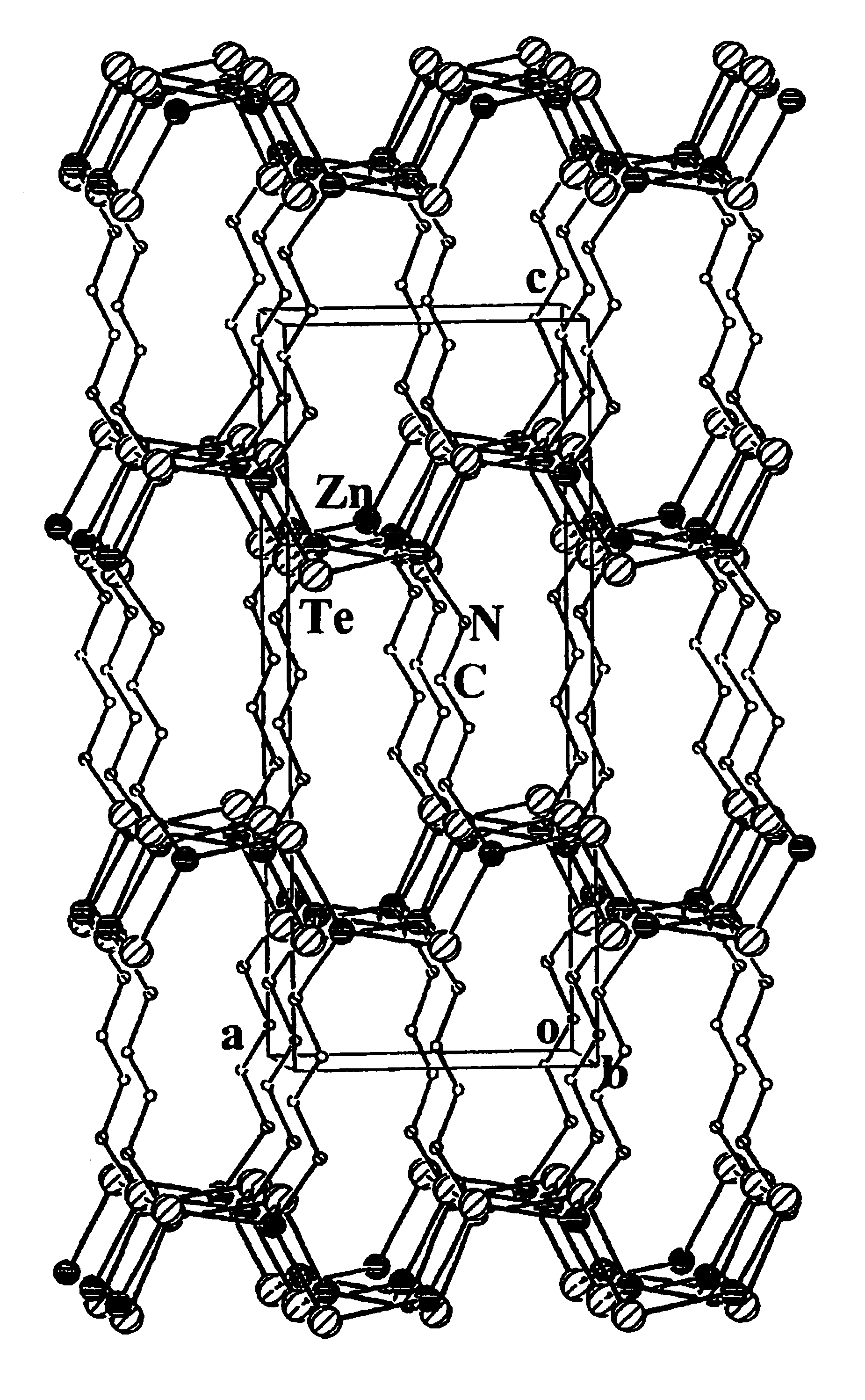
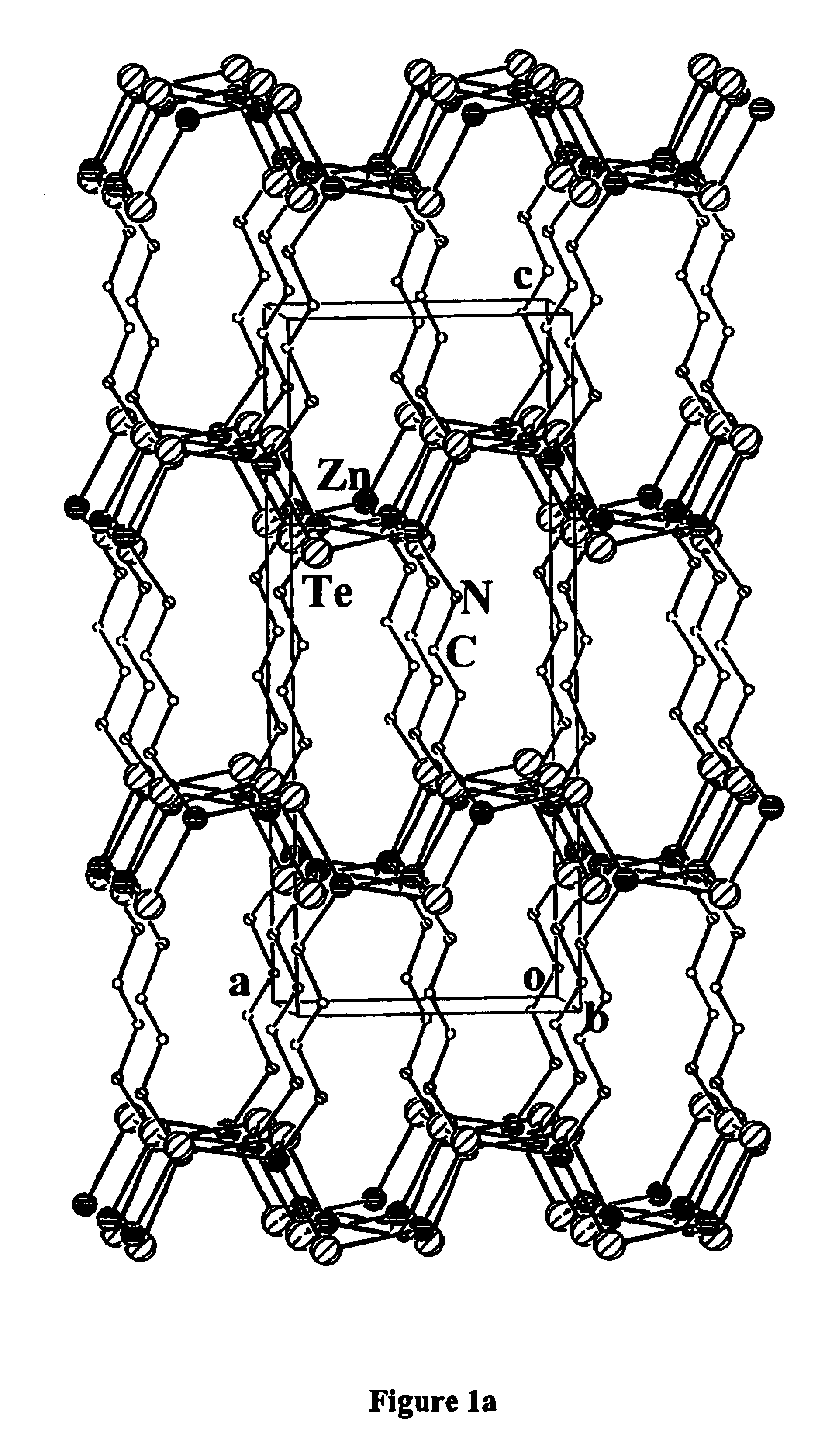
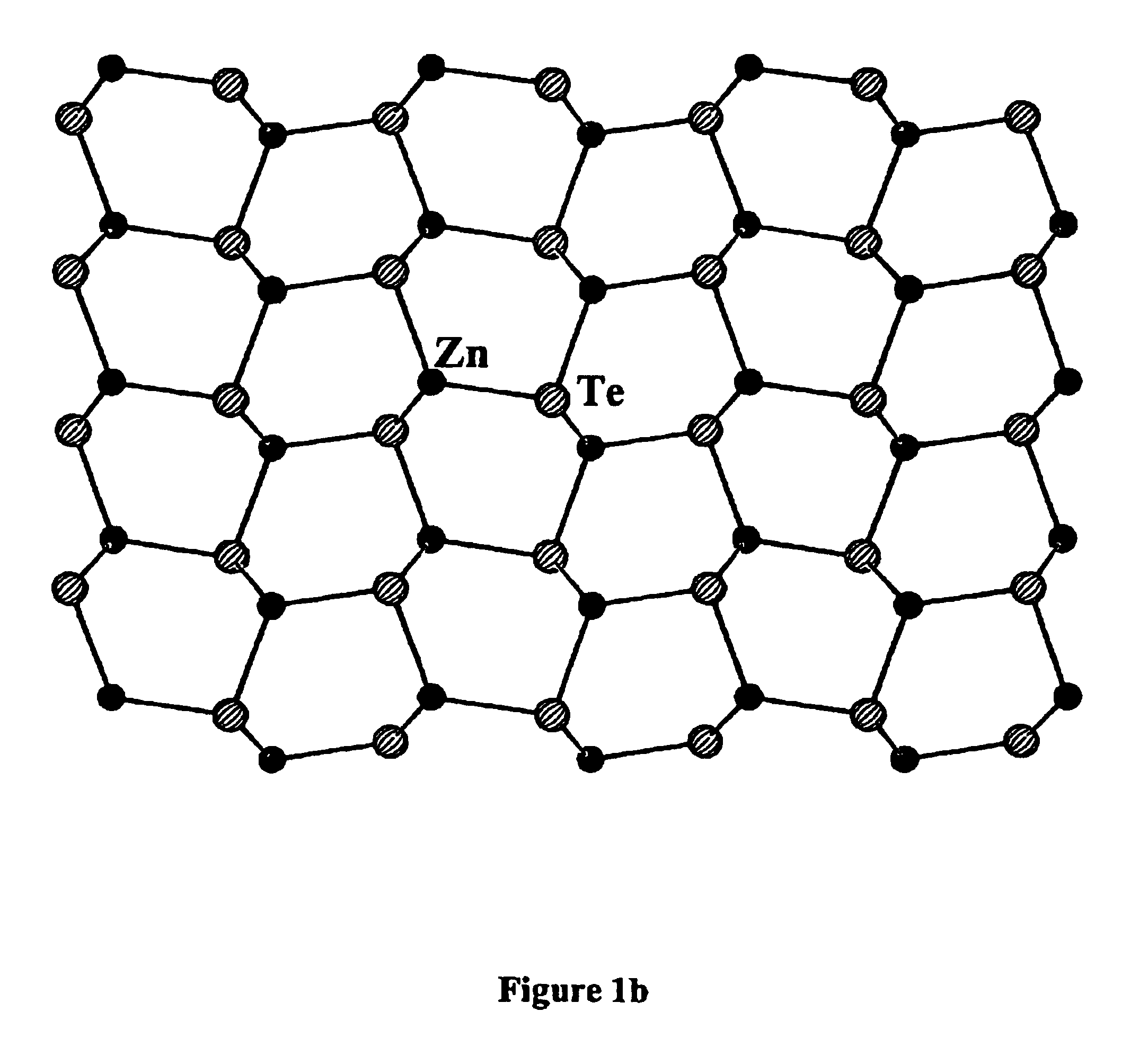
[0006]This need is met by the present invention. Applicants have discovered a new type of quantum confined nanostructures that are not only capable of modifying optical, electronic and other properties of a semiconductor on the same large scale as colloidal dots, but also present uniform structures that are particularly advantageous to device making. Compounds of the present invention are covalent or coordinate bonded organic-inorganic hybrid materials with a uniform, periodic nanostructure exhibiting significant quantum confinement effects.
[0018]The alternating semiconductor and organic layers of the hybrid material of the present invention, prepared by the methods described herein, mimic a superlattice structure. However, unlike the conventional semiconductor superlattices where the band offset introduces only a weak confinement, the insulating organic layer will impose a strong confinement on the semiconductor layer, giving rise to a large variation with respect to the bulk semiconductor properties. In addition, the hybrid organic-inorganic nature of the composites of the present invention provides advantages, features and properties that are important for the miniaturization of electronic and optical devices. Representative features include superior electronic and optical properties, as well as rigidity and stability provided by the inorganic component, and high processibility, flexibility, weight reduction and structural diversity provided by the organic component. Therefore, according to another aspect of the present invention, a semiconductor device is provided containing multiple layers of the crystalline organic-inorganic hybrid compounds of the present invention. The semiconductor devices of the present invention are fabricated by known techniques.

Problems solved by technology

The great challenge, however, is to generate uniformly sized dots and to organize them into periodic arrays in order to obtain sharp line width, and control over intensity and other optical properties.
Self-assembled strain dots have some uniform structures, but their ability to change optical properties is severally limited.
This substantially restricts their uses.

Method used


Image

  • Hybrid nanostructured materials based in II-VI semiconductors
  • Hybrid nanostructured materials based in II-VI semiconductors
  • Hybrid nanostructured materials based in II-VI semiconductors

Examples


example 1

Preparation of [α-ZnTe(Ethylenediamine)1 / 2] I

[0042]To a 23 mL acid digestion bomb was charged 0.272 g ZnCl2 (2 mmol), 0.128 g Te (1 mmol) and 6 mL ethylene-diamine. The mixture was allowed to react at 200° C. for a period of three days. A solid product was collected, washed with 30 and 80% ethanol, and then dried in anhydrous ethyl ether giving brownish column-like crystals of the title compound in 90.0% yield.

example 2

Preparation of [β-ZnTe(Ethylenediamine)1 / 2] II

[0043]A reaction mixture of 0.595 g Zn(NO3)2.6H2O (2 mmol), 0.128 g Te (1 mmol), and ethylenediamine (6 mL, 90 mmol) was heated in a 23 mL acid digestion bomb at 190° C. for three days. A solid product was collected, washed with 30 and 80% ethanol, and dried in anhydrous ethyl ether, affording brownish platelike crystals of the title compound (92.4% yield).

example 3

Preparation of [ZnTe(1,3-Propanediamine)1 / 2] III

[0044]The title compound was prepared as in Example 2 with the exception that 1,3-propanediamine (5 mL, 60 mmol) was used in place of ethylenediamine and the reaction temperature was 200° C. The title compound was obtained in 91.3% yield.


PUM


Abstract

Hybrid crystalline organic-inorganic quantum confined systems are disclosed, which contain alternating layers of a bifunctional organic ligand and a II-VI semiconducting chalcogenide, wherein the semiconducting chalcogenide layers contain chalcogenides have the formula MQ, in which M is independently selected from II-VI semiconductor cationic species and Q is independently selected from S, Se and Te; and the bifunctional organic ligands of each organic ligand layer are bonded by a first functional group to an element M of an adjacent II-VI semiconducting chalcogenide layer and by a second functional group to an element M from the adjacent opposing II-VI semiconducting chalcogenide layer, so that the adjacent opposing II-VI semiconducting chalcogenide layers are linked by the bifunctional organic ligands of the organic ligand layers. Optical absorption experiments show that these systems produce a significant blue shift in their optical absorption edges, 1.2-1.5 eV, compared to a shift of 1.0 electron volt by the best grown II-VI or II-V semiconducting quantum colloidal dots. In addition, the II-VI confined layers in these systems possess a perfectly periodic arrangement.

Description

[0001]This application claims the benefit of Provisional application Ser. No. 60 / 282,967, filed Apr. 11, 2001.GOVERNMENT SUPPORT [0002]The development of this invention was supported in part by National Science Foundation Grant DMR-0094872. The Government has certain rights in the invention.<?insert-end id="INS-S-00002" ?>BACKGROUND OF THE INVENTION[0003]The present invention relates to organic-inorganic hybrid composites which have unique and useful electronic and optical properties. More specifically, the invention relates to II-VI semiconducting chalcogenides with modified structures and properties based upon the incorporation of organic components via coordination or covalent bonds.[0004]Group II-VI semiconducting chalcogenide compounds such as CdTe and ZnSe are of great interest currently for use in semiconductor devices because of their relatively wide band gaps. Semiconductor nanostructures with uniform arrangement, such as periodic arrays of quantum dots, are necessary...

Claims


Application Information

Patent Timeline
IPC IPC(8): H01L31/00C07F13/00H01L51/30
CPCC07F13/005H10K85/00
Inventor LI, JINGHUANG, XIAOYING
Owner RUTGERS THE STATE UNIV
Learn More