Electronic device comprising an organic semiconducting material
a semiconducting material and electronic device technology, applied in semiconductor devices, solid-state devices, other domestic articles, etc., can solve the problems of reduced contact resistance, difficult injection of etl with very high lumo, etc., to achieve good lumo position of organic light-emitting devices, good conductivity and charge carrier mobility, and high thermal stability
- Summary
- Abstract
- Description
- Claims
- Application Information
AI Technical Summary
Benefits of technology
Problems solved by technology
Method used
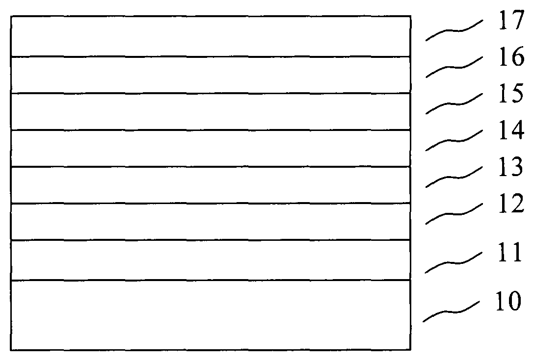
Image


Examples
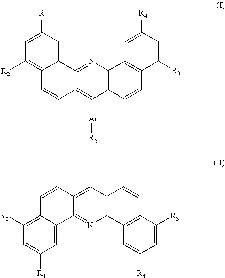
example 1
Synthesis of
[0064]
[0065]First Step:
[0066]Synthesis of 2-benzylidene-3,4-dihydronaphthalen-1(2H)-one (1). All manipulations were carried out in air, without any further purification of commercial solvents / chemicals.
[0067]
[0068]A 250 mL flask was charged with tetralone (4 g, 27.4 mmol) and benzaldehyde (3.88 g, 36.6 mmol). This was dissolved in warm tetrahydrofuran (15 mL), and to this yellow solution was slowly added a 4 wt % solution of KOH in methanol (125 mL). The reaction was stirred for 4 days at room temperature. The solvent was then removed under reduced pressure, and it was poured into 150 mL of water and extracted with methylene chloride. The organic extract was dried over magnesium sulfate and filtered, and the solvent was removed at reduced pressure to afford 4.1 g (64%) as white powder.
[0069]NMR: 1H NMR (500 MHz, CD2Cl2) δ 8.01 (dd, J=64.7, 65.4, 2H), 7.71-6.92 (m, 8H), 3.39-2.64 (m, 4H).
[0070]Second Step:
[0071]Synthesis of 7-phenyl-5,6,8,9-tetrahydrodibenzo[c,h]acridine ...
example 2
Synthesis of
[0079]
[0080]First Step:
[0081]Synthesis of (E)-2-(4-bromobenzylidene)-3,4-dihydronaphthalen-1(2H)-one (4). All manipulations were carried out in air, without any further purification of commercial solvents / chemicals.
[0082]
[0083]A 250 mL flask was charged with tetralone (3.22 g, 22 mmol) and 4-bromobenzaldehyde (5.3 g, 28.6 mmol). This was dissolved in warm tetrahydrofuran (12 mL), and to this yellow solution was slowly added a 4 wt % solution of KOH in methanol (100 mL). The reaction was stirred for 4 days at room temperature. The mixture was concentrated and reduced to approx 10% vol. The residue was filtered and washed with MTBE (3*50 mL), dried, to afford a light yellow powder (6.61 g, 96%).
[0084]Second Step:
[0085]Synthesis of 7-(4-bromophenyl)-5,6,8,9-tetrahydrodibenzo[c,h]acridine (5). All manipulations were carried out under argon.
[0086]
[0087]4 (6.54 g, 20.9 mmol) and tetralone (2.93 g, 20.0 mmol) are introduced in a flask together with BF3.Et2O (3 mL, 23.7 mmol). T...
example 3
Synthesis of
[0099]
[0100]First Step:
[0101]Synthesis of (E)-2-(3-bromobenzylidene)-3,4-dihydronaphthalen-1(2H)-one (8). All manipulations were carried out in air, without any further purification of commercial solvents / chemicals.
[0102]
[0103]A 250 mL flask was charged with tetralone (5.2 g, 35.6 mmol) and 3-bromobenzaldehyde (8.51 g, 56 mmol). This was dissolved in warm tetrahydrofuran (20 mL), and to this yellow solution was slowly added a 4 wt % solution of KOH in methanol (160 mL). The reaction was stirred for 4 days at room temperature. The mixture was concentrated and reduced to approx 10% vol. The residue was filtered and washed with MTBE (3*50 mL), dried, to afford a light yellow powder (10.3 g, 92%).
[0104]NMR: 1H NMR (500 MHz, CD2Cl2) δ 8.01 (dd, J=64.7, 65.4, 2H), 7.71-6.92 (m, 8H), 3.39-2.64 (m, 4H).
[0105]Second Step:
[0106]Synthesis of 7-(3-bromophenyl)-5,6,8,9-tetrahydrodibenzo[c,h]acridine (9). All manipulations were carried out under argon.
[0107]
[0108]4 (10.2 g, 32.6 mmol)...
PUM
| Property | Measurement | Unit |
|---|---|---|
| HOMO energy level | aaaaa | aaaaa |
| LUMO energy | aaaaa | aaaaa |
| energy level | aaaaa | aaaaa |
Abstract
Description
Claims
Application Information
 - R&D
- Intellectual Property
- Life Sciences
- Materials
- Tech Scout
- Unparalleled Data Quality
- Higher Quality Content
- 60% Fewer Hallucinations
Browse by: Latest US Patents, China's latest patents, Technical Efficacy Thesaurus, Application Domain, Technology Topic, Popular Technical Reports.
© 2025 PatSnap. All rights reserved.Legal|Privacy policy|Modern Slavery Act Transparency Statement|Sitemap|About US| Contact US: help@patsnap.com