Method for improving the bonding strength between nickel or nickel alloy cast layers in laminated micro devices

A combination strength and micro-device technology, which is applied in chemical instruments and methods, microstructure technology, microstructure devices, etc., can solve the problems that the requirements of high bonding strength cannot be fully met, the process reproducibility is poor, and the bonding strength between layers is low.

Inactive Publication Date: 2008-05-14
SHANGHAI JIAO TONG UNIV
View PDF3 Cites 0 Cited by
  • Summary
  • Abstract
  • Description
  • Claims
  • Application Information

AI Technical Summary

Problems solved by technology

Although this method is simple to operate and does not require special equipment, the overall idea does not deviate from the traditional processing method, the interlayer bonding strength is still low, and the process reproducibility is poor, which requires high bonding strength between laminated nickel or nickel alloy casting layers. still not fully satisfied

Method used


Image

  • Method for improving the bonding strength between nickel or nickel alloy cast layers in laminated micro devices

Examples


Embodiment 1

[0021] Embodiment 1 electroforming nickel to make double-layer microgear

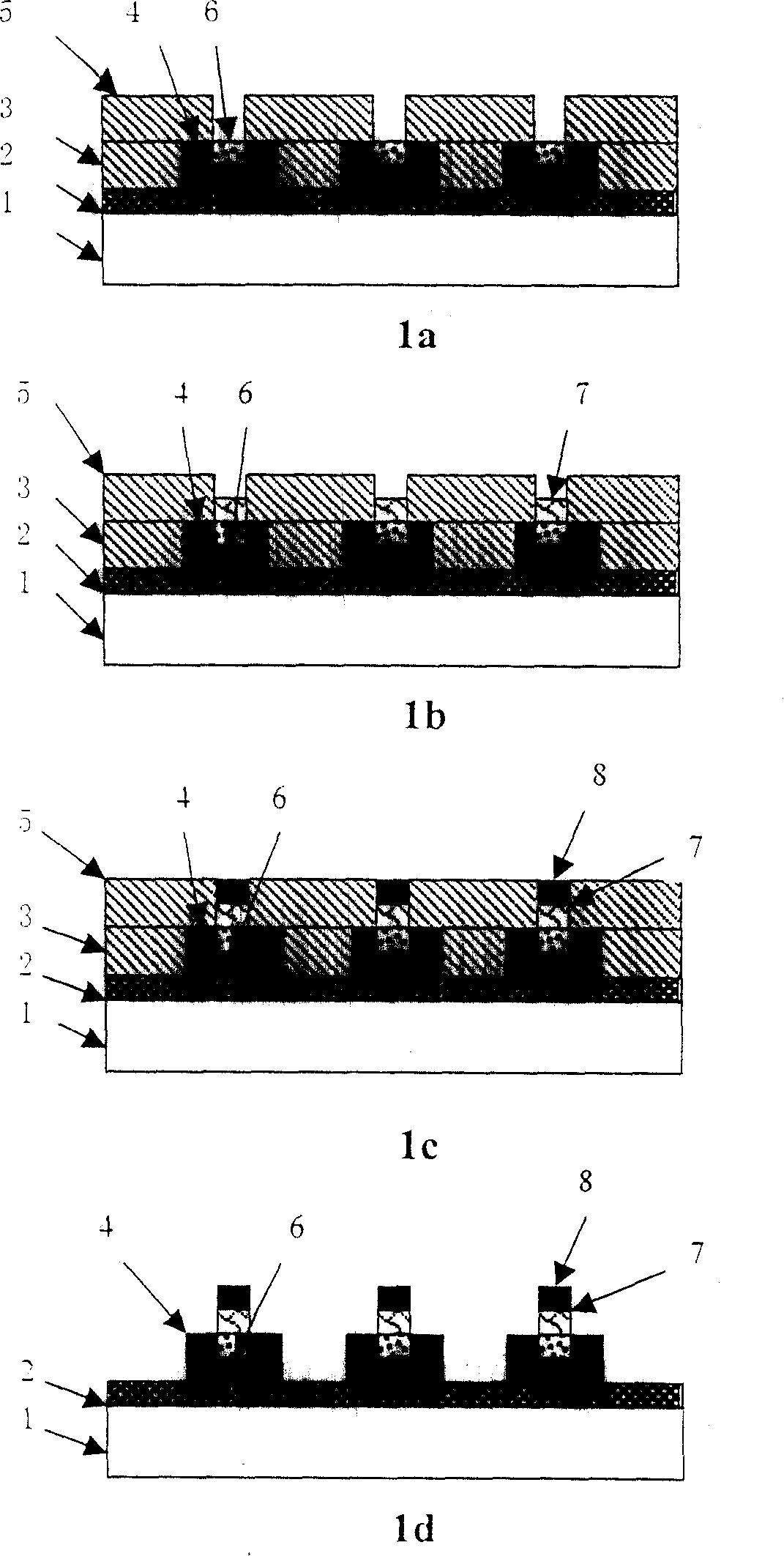
[0022] Such as figure 1 shown, according to figure 1 For implementation, due to the special requirements on the structure of the double-layer micro-gear, UV-LIGA technology is used for micro-processing. That is, on the glass substrate 1, the Cr / Cu seed layer 2 is sputtered, the first layer of photoresist 3 is formed by spraying glue and photolithography, and then the first layer of nickel casting is obtained after mask electroforming and polishing. Layer 4; on it, a second layer of photoresist 5 is formed by lithography and photolithography; then activation-AC transition plating is performed. The treatment liquid this time uses NiSO 4 ·6H 2 O 120g / l, NiCl 2 ·6H 2 O 120g / l, HCl 100g / l and sodium 1,3,6-naphthalenetrisulfonate 0.05g / l, the pH was adjusted to 1.0, and the treatment temperature was 45°C.

[0023] 1) if figure 1 a cathode and anode alternate etching treatment: anode current density 7A...

Embodiment 2

[0027] Embodiment 2 Electroformed double-layer nickel-iron alloy

[0028] Thickness 0.3mm, area 1.5×1.5cm 2 Experiments on the bonding force of electroformed double-layer nickel-iron alloys on copper sheets. After the copper substrate 1 is degreased and polished, a 100 μm nickel-iron alloy cast layer 4 is plated in a sulfate-based nickel-iron alloy electroplating solution. After being placed in the atmosphere for 24 hours, secondary nickel-iron alloy electroforming is performed. The solution used in the activation treatment is made of NiCl 2 ·6H 2 O 100g / l, FeCl 2 4H 2 O 10g / l, HCl 20g / l and sodium dodecyl sulfonate 0.01g / l, adjust the pH to 1.5, and the temperature is 50°C; immerse the nickel-iron-plated test piece in the above solution for activation treatment.

[0029] first step, such as figure 1 a cathode and anode alternate etching treatment: anode current density 3A / dm 2, pulse period 1ms, cathode current density 1.5A / dm 2 , the pulse period is 1ms, the etching ...

Embodiment 3

[0033] Embodiment 3 Electroformed double-layer nickel

[0034] Thickness 0.3mm, area 1.5×1.5cm 2 Electroformed double-layer nickel adhesion experiments on copper sheets. Firstly, the copper substrate 1 is degreased and polished, and then a nickel casting layer 4 of 100 μm is plated in a nickel sulfamate plating solution, and placed in the atmosphere for 24 hours, followed by secondary nickel electroforming. The solution used in the activation treatment before the secondary electroforming is made of NiCl 2 ·6H 2 O 150g / l, HCl 50g / l and sodium dodecylsulfonate 0.01g / l, the pH is adjusted to 1.2, and the temperature is 50°C; the primary nickel-plated test piece is immersed in the above solution.

[0035] first step, such as figure 1 a cathode and anode alternate etching treatment: anode current density 5A / dm 2 , pulse period 10ms, cathode current density 2.5A / dm 2 , the pulse period is 10ms, the etching time is 5min, and the cathode and anode alternate etching layer 6 is fo...


PUM

PropertyMeasurementUnit
pore sizeaaaaaaaaaa

Abstract

The present invention provides a method to increase inter-layer bond strength of electroformed nickel or nickel alloy lamination micro device. The surface of first Ni forming layer must be transitionally treated by activation-alternate current treatment when the first Ni forming layer is re-electroformed with Ni. The said alternate current treatment is etching with alternate cathodic and anodic current, wherein anodic current density, 3-7 A / dm2, is 2-5 times of cathodic current density, and alternate impulse period is 1-20 ms and etching time 3-7 minutes. During alternate current transition plating treatment, cathodic current keeps unchanged and anodic current is gradually decreased to 1 / 5 of the initial value, and then the treatment is converted into normal direct current plating. Adopting the present invention technology, the inter-layer bond strength can reach 15 -25 Kg / mm2, and inter-layer borderlines are ambiguous, meaning integrated into one piece.

Description

technical field [0001] The invention relates to a method for improving the bonding strength between nickel or nickel alloy cast layers of a laminated micro device, in particular to a micro-electromechanical system (MEMS) based on three-dimensional microstructure processing using electroforming technology to manufacture a The invention relates to a method for a micro-device with a stacked structure of nickel or nickel alloy, which belongs to the technical field of electrochemical machining and forming micro-manufacturing. Background technique [0002] LIGA (the abbreviation of Lithographie, Galvanoformung and Abformung in German) technology is a three-dimensional microstructure three-dimensional processing technology that appeared in the 1980s. technology. The three-dimensional microstructure devices manufactured by this technology not only have a large aspect ratio and fine structure, but also have steep side walls and flat surfaces, and the thickness can reach 500 μm or ev...

Claims


Application Information

Patent Timeline
Patent Type & Authority Patents(China)
IPC IPC(8): C25D1/00C25D5/14C25D5/34B81C5/00B81C99/00
Inventor 汪红赵小林丁桂甫陈迪王志民
Owner SHANGHAI JIAO TONG UNIV
Why Eureka
Try Eureka