Production of hafnium nitride thin-membrane materials from ion beam epitaxial growth apparatus

A technology of epitaxial growth and thin film materials, applied in the field of semiconductors, can solve the problems of expensive raw materials, difficult to purify transition group IVB refractory metal nitrides, etc., and achieve the effect of high-quality chemical ratio

Inactive Publication Date: 2008-10-08
INST OF SEMICONDUCTORS - CHINESE ACAD OF SCI
View PDF4 Cites 1 Cited by
  • Summary
  • Abstract
  • Description
  • Claims
  • Application Information

AI Technical Summary

Problems solved by technology

[0005] The methods currently used to prepare and grow hafnium nitride (HfN) thin films mainly include magnetron sputtering, pulsed laser deposition (PLD), ion beam assisted deposition (IBAD), plasma vapor deposition (PVD), and chemical vapor deposition (CVD). ) and electron beam evaporation, etc., but to prepare and grow hafnium nitride (HfN) thin films suitable for the semiconductor field, the above method still has the following disadvantages: 1) the existing common preparation and growth methods usually have very high requirements on the purity of raw materials High, and high-purity hafnium-containing raw materials are much more expensive than titanium and hafnium-containing raw materials of the same purity
The mass-separated low-energy ion beam epitaxy method has been successful in the growth and preparation of rare earth thin film materials, but there is still little research on how to use this method to grow the transition group IVB refractory metal nitrides with high melting point and difficult to purify. to report

Method used


Image

  • Production of hafnium nitride thin-membrane materials from ion beam epitaxial growth apparatus
  • Production of hafnium nitride thin-membrane materials from ion beam epitaxial growth apparatus
  • Production of hafnium nitride thin-membrane materials from ion beam epitaxial growth apparatus

Examples


preparation example Construction

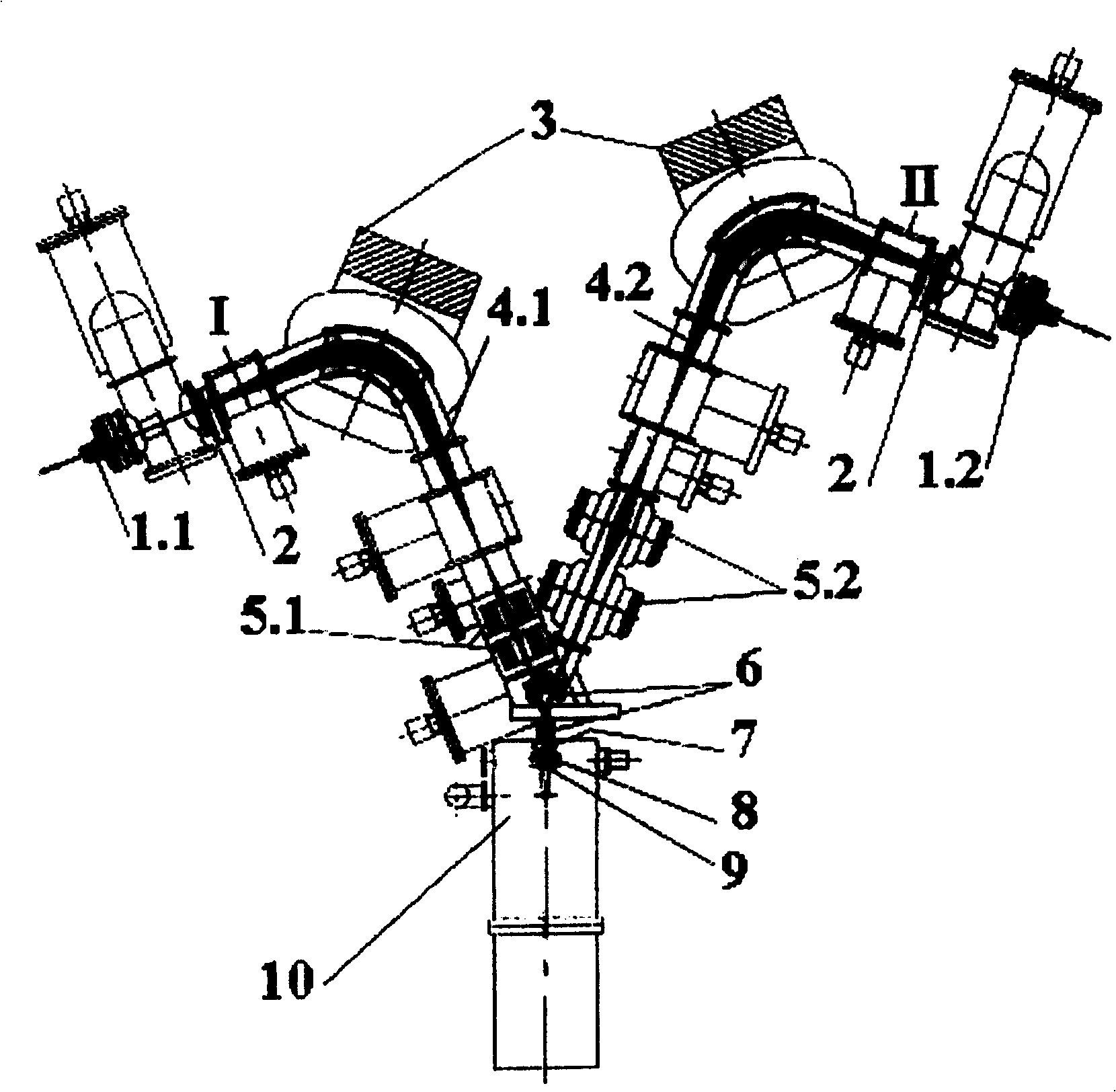
[0071] The preparation of hafnium nitride (HfN) thin film materials is carried out on an ion beam epitaxy system with a double-beam structure, and hafnium chloride (HfCl) with low purity requirements is selected. 4 ) solid powder and nitrogen as the two ion sources of the dual ion beam epitaxy system to generate metal hafnium ions (Hf + ) beam and nitrogen ions (N + ) bundle of raw materials, reducing the cost of raw materials for the preparation and growth of hafnium nitride (HfN) thin film materials;

[0072] Using the mass separation function and ion deceleration function of the ion beam epitaxy growth equipment, the isotopically pure and low-energy metal hafnium ions (Hf + ) beam and nitrogen ions (N + ) beam, and the preparation and growth of thin film materials in an ultra-high vacuum growth chamber without any auxiliary working gas, and realized the high-purity growth of hafnium nitride (HfN) thin films that are difficult to purify;

[0073] Isotopically pure low-ene...

Embodiment

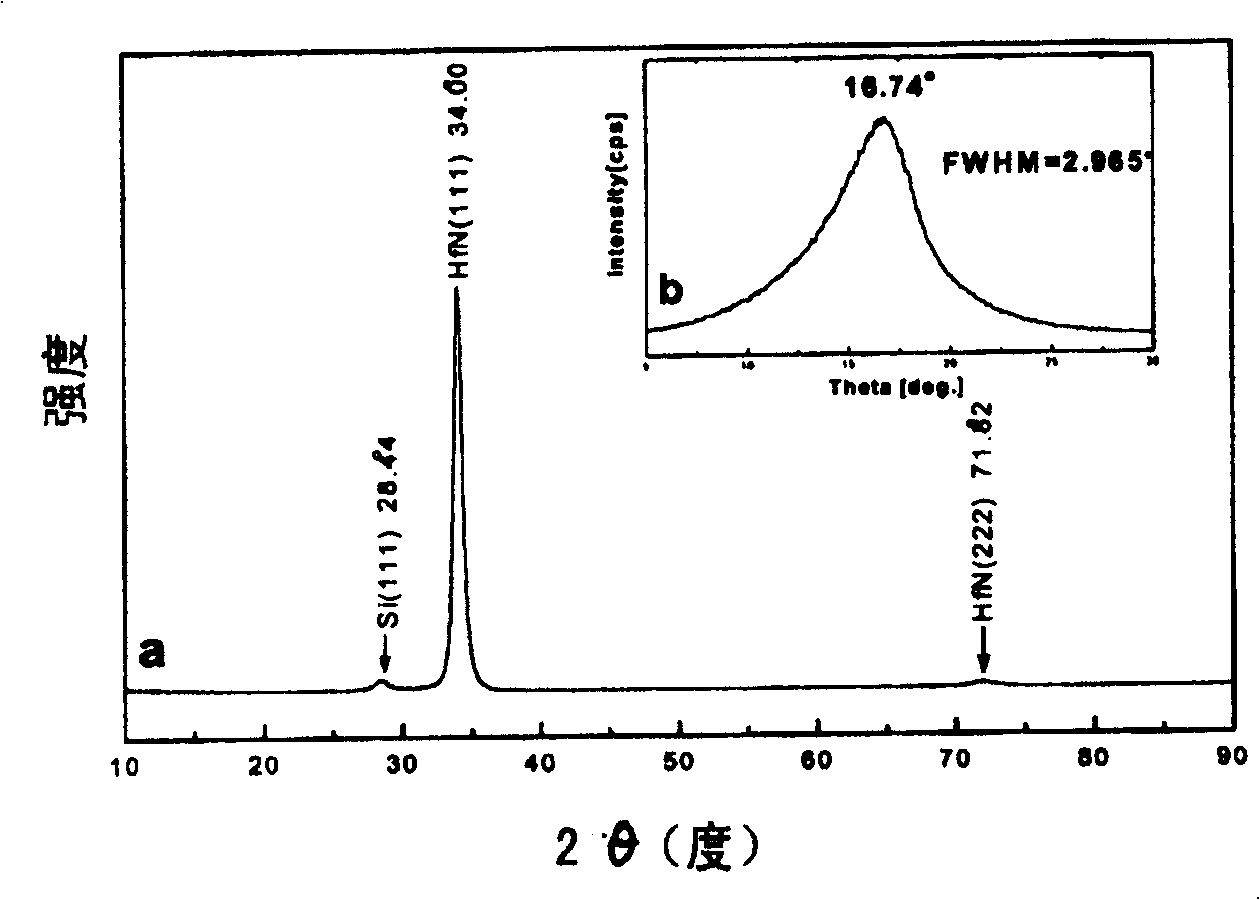
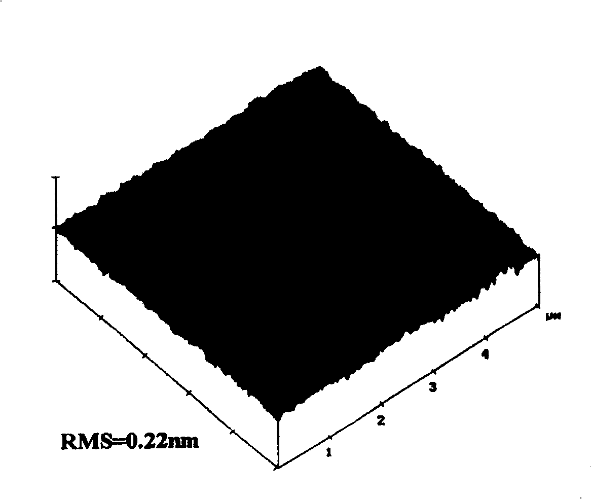
[0081] Concrete embodiment sees the relevant experimental data of table 2 and figure 2 , 3 , 4, 5, 6 experimental results.

[0082] Table 2: Experimental parameters and results of hafnium nitride (HfN) thin film materials prepared by ion beam epitaxy (IBE) growth equipment on Si(111) substrates

[0083]

[0084]

[0085]

[0086]


PUM


Abstract

A method of producing hafnium nitride(HfN) thin-film material by ion beam epitaxy growing equipment. The process includes selecting hafnium tetrachloride (ZrCl4) powder andnitrogen(N2) as the materials of producing low-energy isotope Hf+ ion beam and N+ ion beam ,choosing twoion beams epitaxy growing equipment with mass separation function and Energetic-Ions depositing function, accurate controlling dosage and mixture ratio ,ion energy and growth temperature of the ion beams; obtaining hafnium nitride thin-film with high quality growth and low temperature extension in ultrahigh vacuum chamber. It's a practical and economical method for producing hafnium nitride thin-film material in semiconductor domain owing to its convenience in growth controlling and optimizing.

Description

technical field [0001] The invention belongs to the technical field of semiconductors, in particular to a method for preparing a hafnium nitride (HfN) film material by using ion beam epitaxy (IBE) growth equipment. Background of the invention [0002] Group IVB refractory metal mononitrogen compounds with sodium chloride (NaCl) structure (B1 type), mainly including titanium nitride (TiN), hafnium nitride (ZrN) and hafnium nitride (HfN), all of which have High melting point, high density, high hardness and bright golden luster, in addition to being a good hard coating and decorative material, it has important applications in cutting tools, spare parts anti-corrosion and anti-wear treatment, decoration, etc., because it also has It has high electrical conductivity, good lattice matching with silicon (Si), and good thermal and chemical stability characteristics. It also has important applications in the field of semiconductor technology, such as silicon-based large-scale integr...

Claims


Application Information

Patent Timeline
Patent Type & Authority Patents(China)
IPC IPC(8): C23C14/22C23C14/48C23C14/06C30B25/02H01L21/3205H01L21/318
Inventor 杨少延柴春林刘志凯陈涌海陈诺夫王占国
Owner INST OF SEMICONDUCTORS - CHINESE ACAD OF SCI
Why Eureka
Try Eureka