A surface plasmon crystal and a preparation method thereof

A technology of surface plasmons and crystals, applied in chemical instruments and methods, colloid chemistry, colloid chemistry, etc., can solve the problems of complex process, large equipment investment, high cost, etc., and achieve low equipment requirements and simple preparation process , low cost effect

Inactive Publication Date: 2009-03-04
NANJING UNIV
View PDF2 Cites 2 Cited by
  • Summary
  • Abstract
  • Description
  • Claims
  • Application Information

AI Technical Summary

Problems solved by technology

Although these technologies have a greater degree of freedom in structure control, the equipment investment and process complexity of these technologies make the sample preparation cycle long and costly.
Although some of the technologies listed above can reduce the spatial structure modulation scale to below the submicron level, in practice, these masking or writing techniques still face great challenges in order to obtain ordered structures at the nanometer or deep submicron scale.

Method used


Image

  • A surface plasmon crystal and a preparation method thereof
  • A surface plasmon crystal and a preparation method thereof
  • A surface plasmon crystal and a preparation method thereof

Examples


Embodiment 1

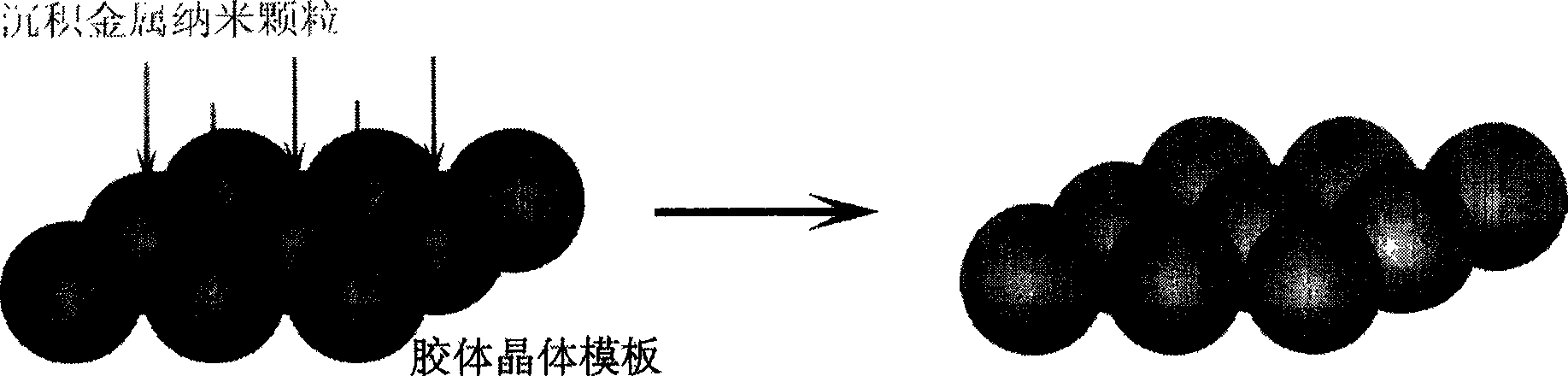
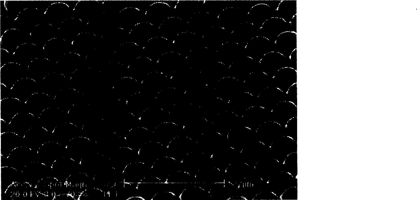
[0018] Embodiment 1: In this example, monodisperse silica microspheres are selected, and the diameter of the silica microspheres is 1580 nm. First, the microspheres are arranged into a hexagonal close-packed array by means of the surface tension in the microchannel (see microsphere self-organization technology, patent ZL 03 1 31989.0). Then, a layer of gold film was deposited on the surface of the microsphere by high vacuum argon ion beam sputtering method, and the deposition amount of gold particles was controlled so that the thickness of the apex of the gold shell layer was 25nm. Since each silica microsphere is covered with a hemispherical gold nanoshell, the hemispherical shell metals are connected to each other, thereby forming equal-diameter silica microspheres in contact with each other and deposited on them. A surface plasmon crystal composed of gold hemispherical shells on the surface.

Embodiment 2

[0019] Embodiment 2: This embodiment is basically the same as Embodiment 1, but the selected target material is a circular silver block with a diameter of 20 mm and a thickness of about 2 mm. Therefore, a surface plasmon crystal composed of equal-diameter silicon dioxide microspheres in contact with each other and a silver hemispherical shell deposited on the surface is formed, and the physical vapor deposition method is a metal thermal evaporation coating method.

Embodiment 3

[0020] Embodiment 3: This embodiment is basically the same as Embodiment 1, but as the medium microsphere array of the substrate, a two-dimensional ordered array of polystyrene microspheres is selected, and what is obtained is made of equal-diameter polystyrene microspheres in contact with each other. The surface plasmon crystal composed of spheres and chromium hemispherical shells deposited on the surface, the thickness of the metal film on the apex of the dielectric microsphere substrate surface is 150nm, and the physical vapor deposition method is laser pulse deposition method.


PUM

PropertyMeasurementUnit
diameteraaaaaaaaaa
thicknessaaaaaaaaaa
diameteraaaaaaaaaa

Abstract

The invention discloses the surface phasmon crystal and preparing method, comprising two-dimensional sequence square dielectric microsphere underlay and metal hemisphere shell membrane under underlay. The metal hemisphere shells are connected with each other, forming the bidimensional cycle ordered structure metal film possessing micropore array. The method comprises the following steps: arraying the sub-micron / micrometer dielectric microsphere to form ordered bidimensional microsphere array; settling metal nanometer particle on bidimensional microsphere with physics vapor deposition method, until forming the continuous metal hemisphere film. The invention has the advantages of novel style structure, adjustable crystal structure parameter, controlling cycle and simple technology.

Description

1. Technical field [0001] The invention relates to a metal nanomaterial and a preparation method thereof, in particular to a surface plasmon crystal and a preparation method thereof. 2. Background technology [0002] Metal nanomaterials and their ordered structures have received worldwide attention due to their rich physical connotations and their direct and potential application value in photonics, electronics, catalysis, biomedicine, and drug delivery. extensive attention and research. Experiments have shown that the shape, size and composition of metal nanoparticles determine their physical and chemical properties. For example, under the action of electromagnetic waves, free electrons on the surface of metal nanoparticles and their ordered structures generate collective oscillations, forming surface plasmons. Coupling and excitation between surface plasmons can significantly improve the efficiency of many optical processes. Surface plasmons can be widely used in fields...

Claims


Application Information

Patent Timeline
Patent Type & Authority Patents(China)
IPC IPC(8): C23C28/02C23C14/22B01J13/00
Inventor 王振林詹鹏董晗孙洁王慧田闵乃本
Owner NANJING UNIV
Why Eureka
Try Eureka