Method for preparing IIB group semiconductor sulfide nano-material

A nanomaterial and semiconductor technology, which is applied in the synthesis field of preparing IIB group sulfide semiconductor nanomaterials, can solve the problems of high reaction temperature requirements, high cost, and difficult to control the morphology of toxic gas products, and achieves low cost, simple operation, Effects that are easy to build

Inactive Publication Date: 2009-05-13
TONGJI UNIV
View PDF3 Cites 0 Cited by
  • Summary
  • Abstract
  • Description
  • Claims
  • Application Information

AI Technical Summary

Problems solved by technology

The above reaction schemes all have problems such as high requirements on reaction temperature (above 600°C), high cost, generation of toxic gas, and difficult control of product morphology.

Method used


Image

  • Method for preparing IIB group semiconductor sulfide nano-material
  • Method for preparing IIB group semiconductor sulfide nano-material
  • Method for preparing IIB group semiconductor sulfide nano-material

Examples


Embodiment 1

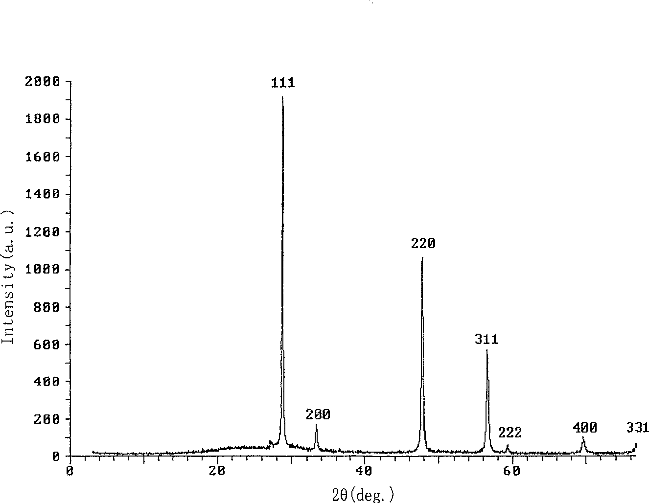
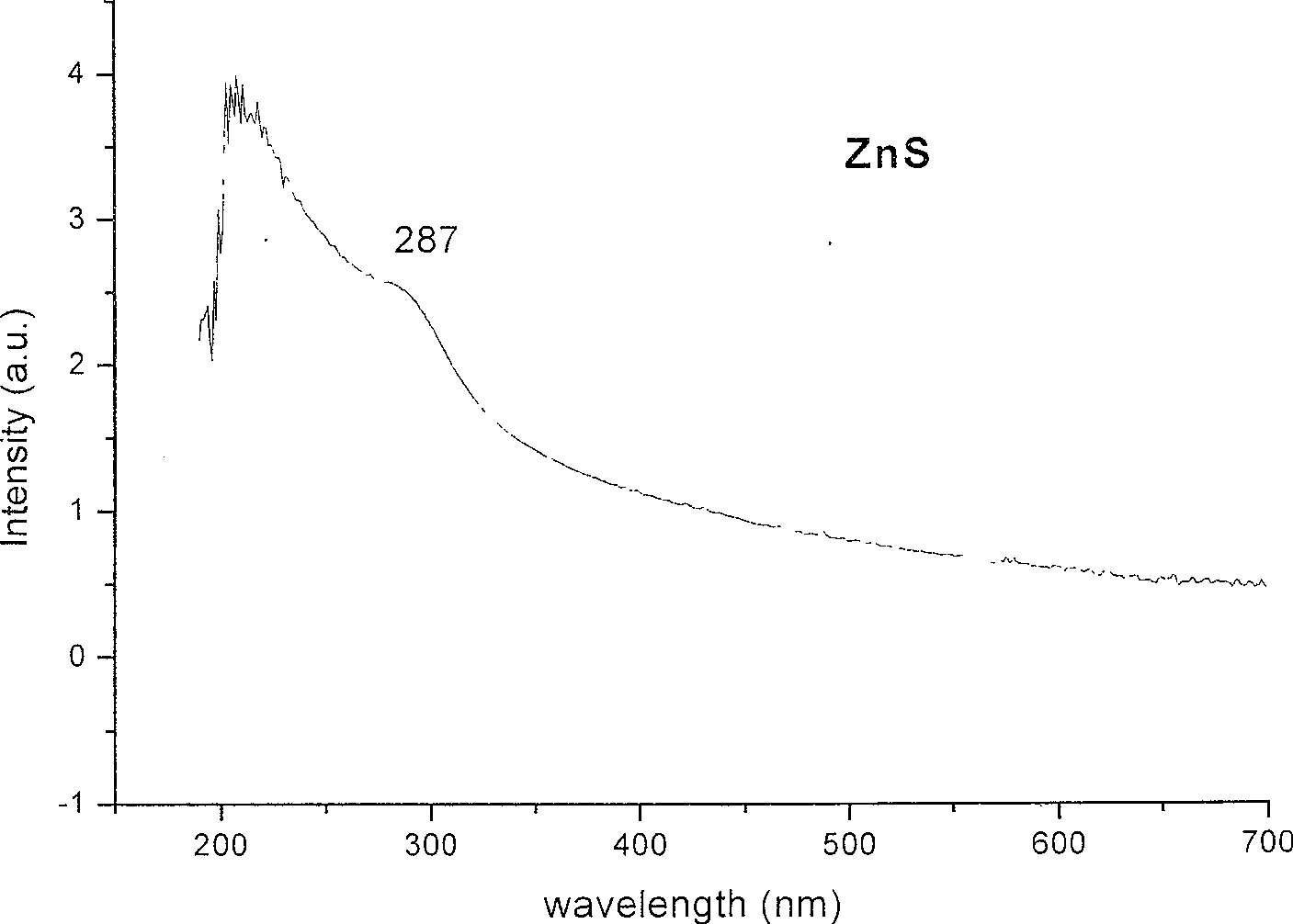
[0020] The first step, weigh 0.010mol zinc powder (analytical pure), sulfur source is 0.010mol Na 2 S (analytical pure). Na 2 S was dissolved in an appropriate amount of distilled water to form a solution.

[0021] In the second step, 0.010mol zinc powder and Na 2 The S solution was placed in a 45mL autoclave lined with polytetrafluoroethylene, and distilled water was added to it to 3 / 4 of the volume of the autoclave. N was then introduced into the reaction solution 2 After removing the dissolved oxygen in the solution, the autoclave was closed, placed in an oven, and heated at 140° C. for 12 hours. After the reaction was finished, the oven was closed, and the autoclave was naturally cooled (gradient temperature drop) to room temperature. Centrifuge at 200rpm with a centrifuge, and suck out the supernatant with a dropper.

[0022] Step 3: Take out the precipitate, wash with water, acetone, and absolute ethanol three times in sequence, and finally store the product in abs...

Embodiment 2

[0024] Replace 0.010mol zinc powder with 0.010mol cadmium powder, reaction temperature is 180 ℃, and sulfur source is 0.015mol thiourea Other conditions and steps are identical with embodiment 1, and the product that obtains is rod-shaped cadmium sulfide nanomaterial, and nanorod diameter is 75nm, about 2.3μm long. And the length and thickness of the rods are relatively uniform. CdS nanorods are cubic phase crystals, and their properties are basically similar to those of ZnS nanocrystals.

Embodiment 3

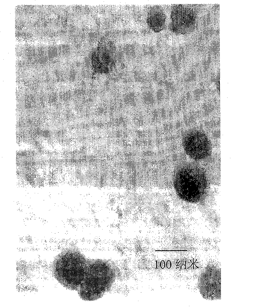
[0026] Replace 0.010mol zinc powder with 0.010mol mercury, the reaction temperature is 200°C, and the sulfur source is 0.020molK 2 S, the reaction time was 24 hours, other conditions and steps were exactly the same as in Example 1, and the product obtained was mercury sulfide particles with an average particle size of 30nm. The ultraviolet absorption peak of HgS nanoparticles has obvious "blue shift" compared with conventional materials, and the results of fluorescence spectrum analysis show that the product has photoluminescence properties.


PUM

PropertyMeasurementUnit
particle sizeaaaaaaaaaa
diameteraaaaaaaaaa
diameteraaaaaaaaaa

Abstract

This invention relates to a method for preparing IIB group semiconductor sulfide nm material, which weighs 0.010molIIB group metal and 0.010-0.020 mol sulfur source first, then dissolves the sulfur source in water to a solution to be transfers to an autoclave with the metal to be filled with distilled water to 3 / 4 of the autoclave to be penetrated with N2 and closed in a bake oven to be heated for 12-48 hours under 140-200deg.C then the temperature is reduced to the room temperature after the reaction, then it is processed by centrifugal separation and cleaned three times with distilled water, propyl alcohol and absolute alcohol, finally the product is kept in the absolute alcohol to be dried naturally to get the approximately spherical IIB group sulfide semiconductor nm material with advanced photoelectric performance.

Description

technical field [0001] The invention relates to a synthesis method for preparing IIB group sulfide semiconductor nanometer materials. Specifically, it refers to a method for controlling the synthesis and preparation of group IIB semiconductor sulfide nanomaterials under hydrothermal conditions by using elemental oxidation and hydrolysis synergistic reactions. Background technique [0002] Group IIB sulfide semiconductor materials are typical broadband semiconductors, and they have broad application prospects in electronics, optics, biology, coatings, medicine and other industries. Many scientific studies have confirmed that when normal substances are processed to extremely small scales, their optical, thermal, electrical, magnetic, mechanical and even chemical properties will also undergo correspondingly significant changes. Due to quantum size effects and surface effects, group IIB sulfide nanomaterials have more excellent optical, electrical, magnetic, and catalytic prope...

Claims


Application Information

Patent Timeline
Patent Type & Authority Patents(China)
IPC IPC(8): H01L21/00C30B29/46B82B3/00
Inventor 陈云吴庆生丁亚平
Owner TONGJI UNIV
Why Eureka
Try Eureka