Modified method for preparing single c-axis oriented zinc oxide film by electrochemical deposition process
A deposition process and electrochemical technology, applied in chemical instruments and methods, single crystal growth, single crystal growth and other directions, can solve the problems of difficult to obtain dense ZnO thin films, control of thin film nucleation density, etc., to simplify the device manufacturing process, Good crystallinity, cost reduction effect
- Summary
- Abstract
- Description
- Claims
- Application Information
AI Technical Summary
Problems solved by technology
Method used
Image
Examples
Embodiment 1
[0051] 1. Prepare zinc nitrate precursor solution. 2.97 g of Zn(NO 3 ) 2 .6H 2 O was dissolved in 100 ml of deionized water to obtain a clear and transparent 0.1 mol / L zinc nitrate precursor solution.
[0052] 2. Use ITO glass as the substrate. Process as follows:
[0053] (1) Ultrasonic washing in detergent solution for 3-5 minutes, and then fully rinsed with deionized water;
[0054] (2) After taking it out, ultrasonically clean it in acetone and alcohol for 3-5 minutes, and then rinse it with deionized water;
[0055] (3) Immerse the cleaned ITO film in dilute hydrochloric acid with a concentration of 5% by volume and corrode it for 10 seconds, rinse thoroughly with deionized water after taking it out, and dry it for later use.
[0056] 3. Film growth. Divided into the following four steps:
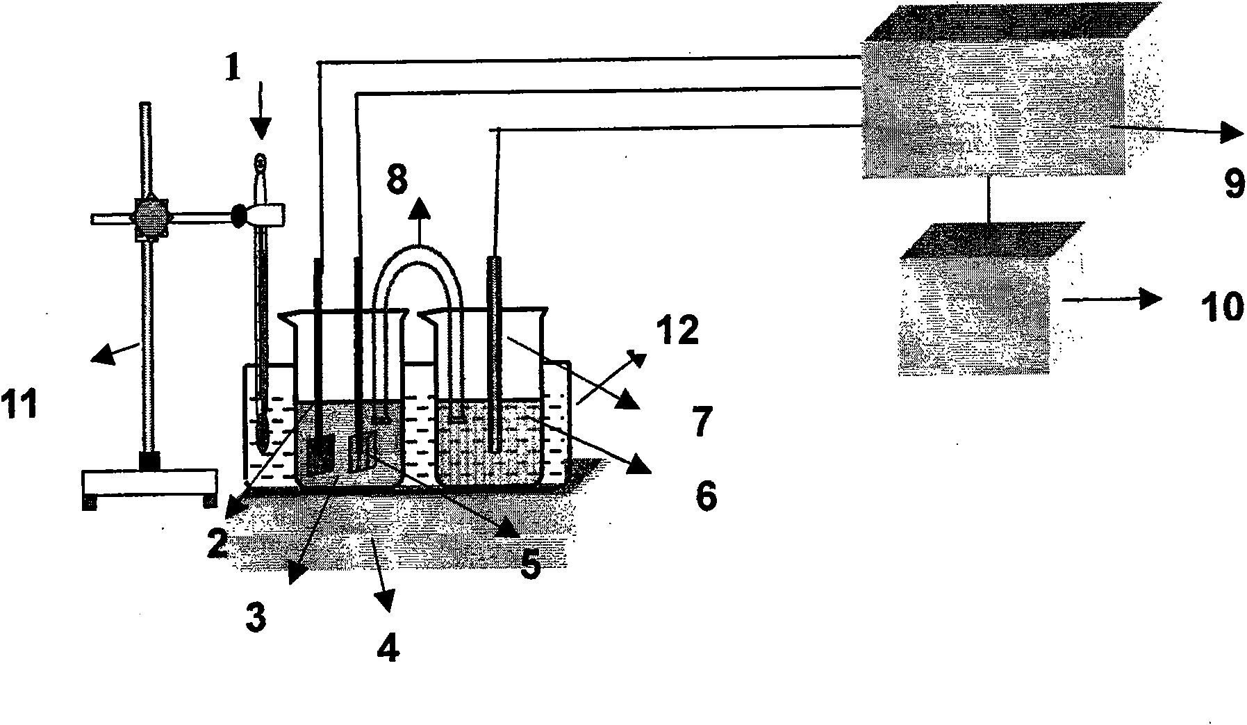
[0057] a. Connect the processed ITO substrate into the attached figure 1 The electrochemical deposition system shown. The basic composition of the electrochemical deposition ...
Embodiment 2
[0063] 1. Prepare zinc nitrate precursor solution. 0.297 g of Zn(NO 3 ) 2 .6H 2 O and 0.85 g NaNO 3
[0064] (sodium nitrate) was dissolved in 100 ml of deionized water to obtain a clear and transparent 0.1 mol / l zinc nitrate precursor solution, and the molar concentration ratio of zinc ions to nitrate ions was 1:11.
[0065] 2. Choose low-resistance single crystal silicon wafer as the substrate. Process as follows:
[0066] (1) At first, the hydrofluoric acid with a volume ratio of 1: 1 cleans the silicon chip under the condition of mechanical stirring for 5 minutes to remove the oxide layer on the surface of the silicon chip;
[0067] (2) After taking it out, ultrasonically clean it in acetone, alcohol, and deionized water for 5 minutes, then rinse it fully with deionized water after taking it out, and dry it for later use.
[0068] 3. Film growth. Divided into the following four steps:
[0069] a. Connect the processed substrate to the electrochemical deposition sy...
PUM
| Property | Measurement | Unit |
|---|---|---|
| particle size | aaaaa | aaaaa |
| thickness | aaaaa | aaaaa |
| particle size | aaaaa | aaaaa |
Abstract
Description
Claims
Application Information


