

Organic electroluminescence device
A technology of luminescence and devices, which is applied in the direction of electroluminescence light sources, electric solid-state devices, electric light sources, etc., can solve the problems of increasing the difficulty of substrate storage, unsuitable for production and practical use, etc., to improve life and mechanical properties, and improve flexibility Sexuality and water oxygen barrier properties, the effect of reducing defects
- Summary
- Abstract
- Description
- Claims
- Application Information
AI Technical Summary
Problems solved by technology
Method used
Image

Examples
preparation example Construction
[0029](1) Preparation of the anode layer: the substrate is a flexible substrate, and the anode layer is deposited on the substrate. The anode can be made of inorganic materials or organic conductive polymers. Inorganic materials are generally metal oxides such as indium tin oxide (ITO), zinc oxide, and tin zinc oxide, or metals with high work functions such as gold, copper, and silver. The optimal choice ITO, usually the square resistance of the ITO film is 50Ω, and the film thickness is generally 150nm. The organic conductive polymer is preferably a material in polythiophene / sodium polyvinylbenzenesulfonate (PEDOT:PSS) and polyaniline (PANI) ;
[0030] (2) Cleaning of the substrate with pre-engraved anodes: the transparent conductive flexible substrate is cleaned by lye spray and deionized water ultrasonic method, after cleaning, it is placed under an infrared lamp for drying, and then the dried The substrate is pretreated by ultraviolet ozone cleaning and low-energy oxygen ...
Embodiment 1
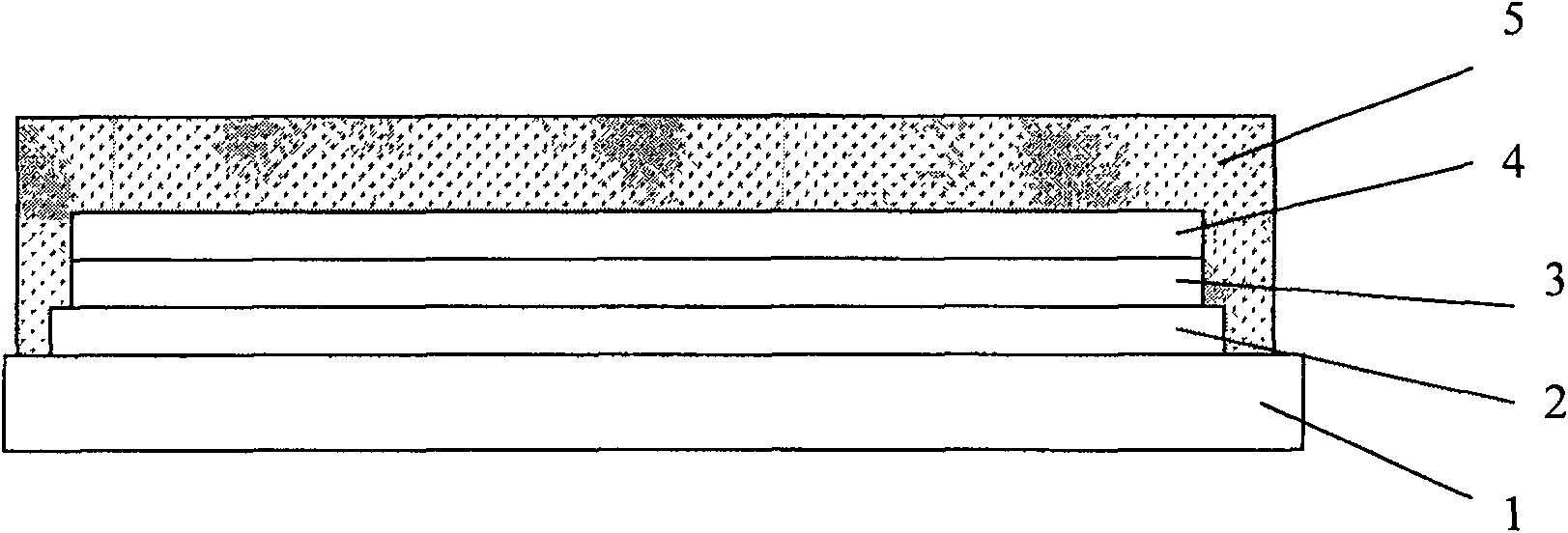
[0041] OLED / Thick Film: Desiccant Particles
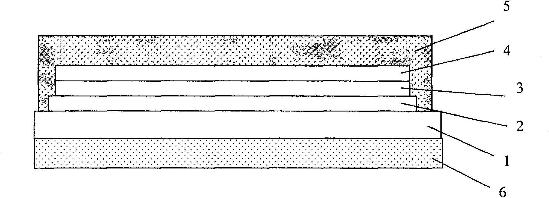
[0042] The schematic diagram of the device structure is as figure 1 1 is the substrate of the OLED device, 2 is the anode of the OLED device, 3 is the organic functional layer of the OLED device, 4 is the cathode layer of the OLED device, and 5 is the thick film layer in the packaging structure of the OLED device.
[0043] The specific structure of the device:
[0044] PET substrate / ITO / NPB / Alq 3 / Mg:Ag / Polymethylmethacrylate: CaO
[0045] (1) Cleaning of PET substrates pre-engraved with ITO: use lye spray and deionized water ultrasonic methods to clean the transparent conductive substrates, place them under infrared lamps for drying after cleaning, and then dry the dried ITO glass is pretreated by ultraviolet ozone cleaning and low-energy oxygen ion beam bombardment. The ITO film on the conductive substrate is used as the anode layer of the device. The square resistance of the ITO film is 50Ω and the film thickness is 150nm;
...
Embodiment 2
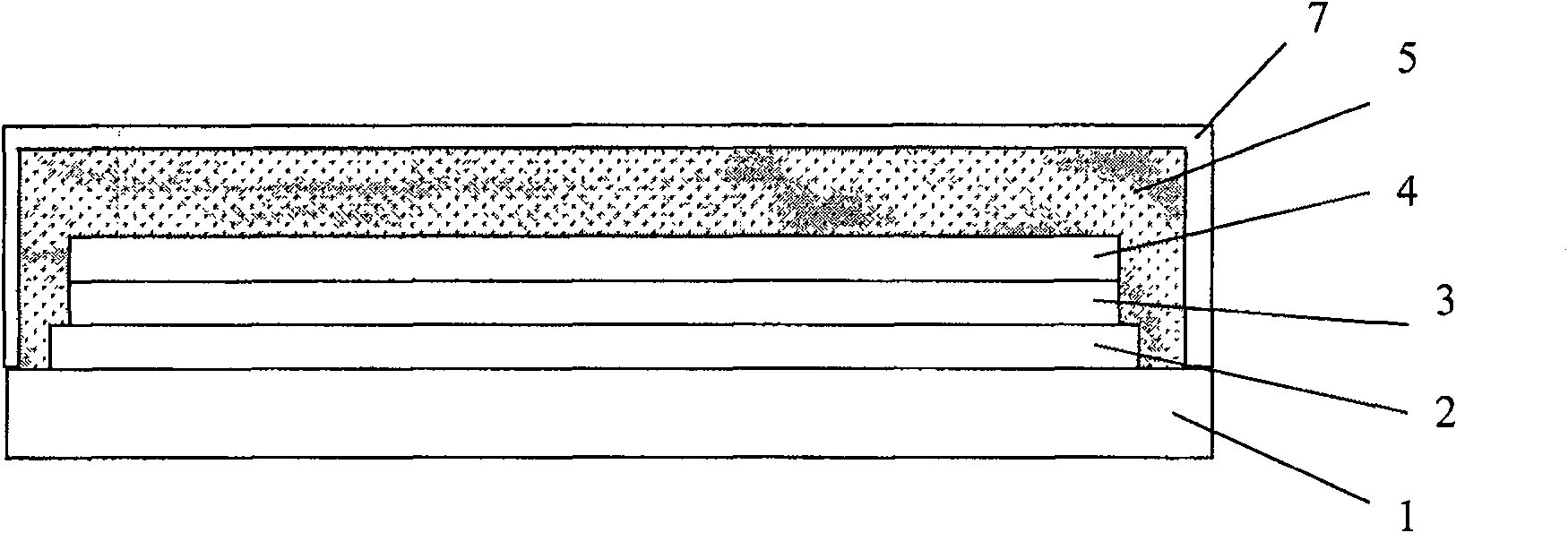
[0050] OLED / Thick Film / Desiccant Particles / Thick Film
[0051] The specific structure of the device:
[0052] PES substrate / ITO / NPB / Alq 3 / Mg:Ag / phenolic resin / sodium / UV glue
[0053] Steps (1)-(3): Prepare the same as (1)(2)(3) in Example 1, and use PES as the substrate material of the OLED device;
[0054] (4) Preparation of encapsulation layer: take out the vapor-deposited device from the vacuum chamber, and transfer it to an environment where water and oxygen are removed to prepare the encapsulation layer. First, prepare a layer of heat-curing adhesive phenolic resin on the metal layer of the OLED device by scraping the film, with a thickness of about 400 μm, and then sprinkle spherical metal Na on it to form a discontinuous distribution. The average size of Na particles is about 10 μm. , and then heat the phenolic resin to about 40°C for 10 minutes to cure it; finally, spin-coat UV glue (UV STRCTL 352, Loctite Company) on the surface of metal Na, and use ultraviolet li...
PUM
| Property | Measurement | Unit |
|---|---|---|
| thickness | aaaaa | aaaaa |
| size | aaaaa | aaaaa |
| thickness | aaaaa | aaaaa |
Abstract
Description
Claims
Application Information