

A method for making the carbon nano tube electronic part
A technology for carbon nanotubes and electronic devices, applied in the field of preparing carbon nanotube electronic devices, can solve the problems of high cost, need for instruments, slow speed, etc., and achieve the effects of low cost, mild operating conditions and high yield
- Summary
- Abstract
- Description
- Claims
- Application Information
AI Technical Summary
Problems solved by technology
Method used
Image

Examples
Embodiment 1
[0083] Embodiment 1: adopt Au / Cr to be the carbon nanotube two-terminal device and field-effect transistor that electrode material is made
[0084] The detailed process of preparation is:
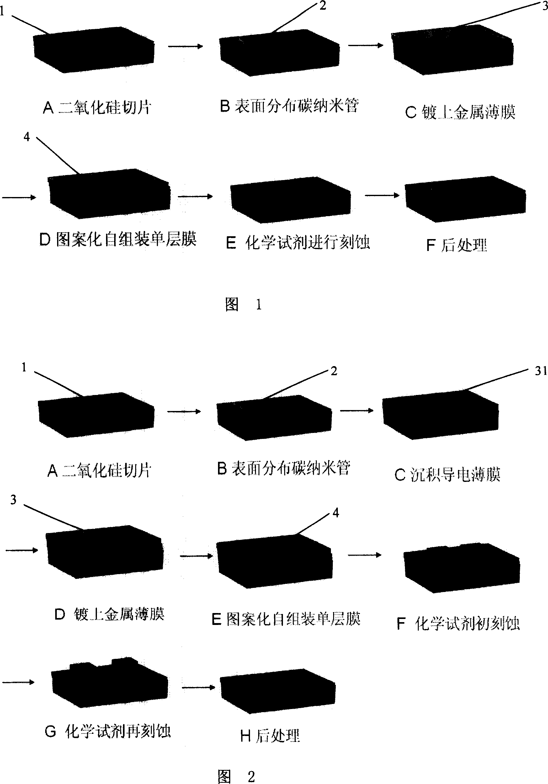
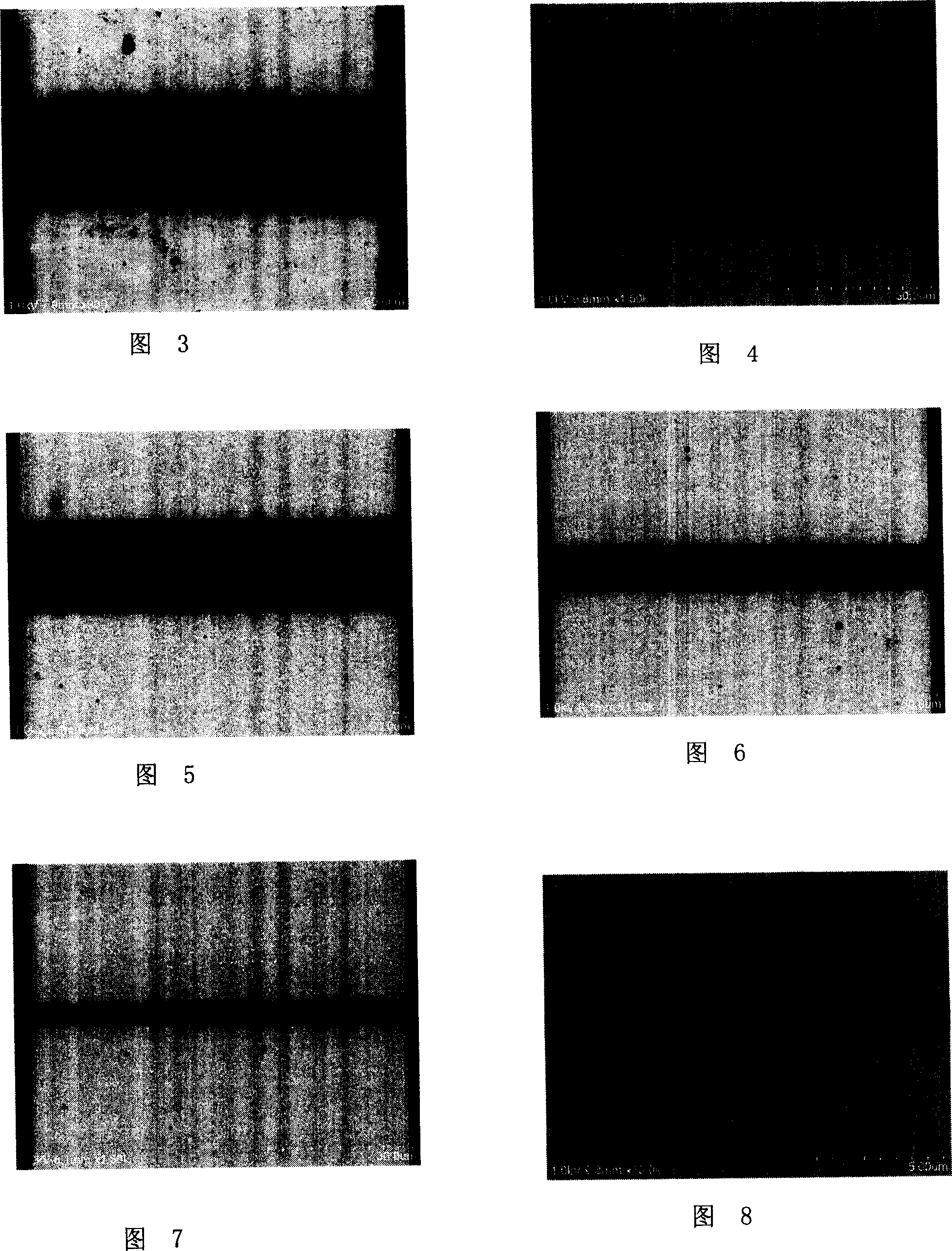
[0085] 1) Directly grow ultra-long carbon nanotubes on the surface of the silica substrate;
[0086] Grow ultra-long carbon nanotubes on the surface of the silica substrate, with a length ranging from a few microns to about one centimeter; the growth temperature is 800-1000 degrees Celsius; the growth time is more than 10 minutes; the carbon source uses ethanol; hydrogen is used as the reducing agent; high Pure argon was used as the carrier gas.
[0087] 2) Coated with metal film
[0088] Thermal evaporation can be used to plate a metal film on the surface of the silicon dioxide substrate distributed with carbon nanotubes: first coat a layer of chromium with a thickness of about 10 nm, and then coat a layer of gold with a thickness of about 80 nm. The thickness of the metal film can be c...
Embodiment 2
[0096] Embodiment 2: adopt Au / Ti as the carbon nanotube two-terminal device and field-effect transistor that electrode material is made
[0097] The detailed process of preparation is:
[0098] 1) Directly grow ultra-long carbon nanotubes on the surface of the silica substrate;
[0099] Grow ultra-long carbon nanotubes on the surface of the silica substrate, with a length ranging from a few microns to about one centimeter; the growth temperature is 800-1000 degrees Celsius; the growth time is more than 10 minutes; the carbon source uses ethanol; hydrogen is used as the reducing agent; high Pure argon was used as the carrier gas.
[0100] 2) Coated with metal film
[0101] Thermal evaporation can be used to plate a metal film on the surface of the silicon dioxide substrate distributed with carbon nanotubes: first coat a layer of titanium with a thickness of about 10 nm, and then coat a layer of gold with a thickness of about 40-80 nm. The thickness of the metal film can be c...
Embodiment 3
[0109] Embodiment 3: adopt Pd / Ti as the carbon nanotube two-terminal device and field-effect transistor that electrode material is made
[0110] The detailed process of preparation is:
[0111] 1) Directly grow ultra-long carbon nanotubes on the surface of the silica substrate;
[0112] Grow ultra-long carbon nanotubes on the surface of the silica substrate, with a length ranging from a few microns to about one centimeter; the growth temperature is 800-1000 degrees Celsius; the growth time is more than 10 minutes; the carbon source uses ethanol; hydrogen is used as the reducing agent; high Pure argon was used as the carrier gas.
[0113] 2) Coated with metal film
[0114] Magnetron sputtering can be used to plate a metal film on the surface of the silicon dioxide substrate distributed with carbon nanotubes: first coat a layer of titanium with a thickness of about 10nm, and then coat a layer of palladium with a thickness of about 90nm. The thickness of the metal film can be ...
PUM
| Property | Measurement | Unit |
|---|---|---|
| thickness | aaaaa | aaaaa |
Abstract
Description
Claims
Application Information