

Novel piezoresistance type pressure pickup and method for making same
A pressure sensor, piezoresistive technology, applied in the direction of fluid pressure measurement by changing ohmic resistance, and measurement of the property and force of piezoresistive materials, which can solve the problems of large differences in sensor performance, low sensor response speed, and difficult implementation Stress film thickness consistency and other issues, to achieve the consistency of product performance guarantee, eliminate metal connection, high sensitivity effect
- Summary
- Abstract
- Description
- Claims
- Application Information
AI Technical Summary
Problems solved by technology
Method used
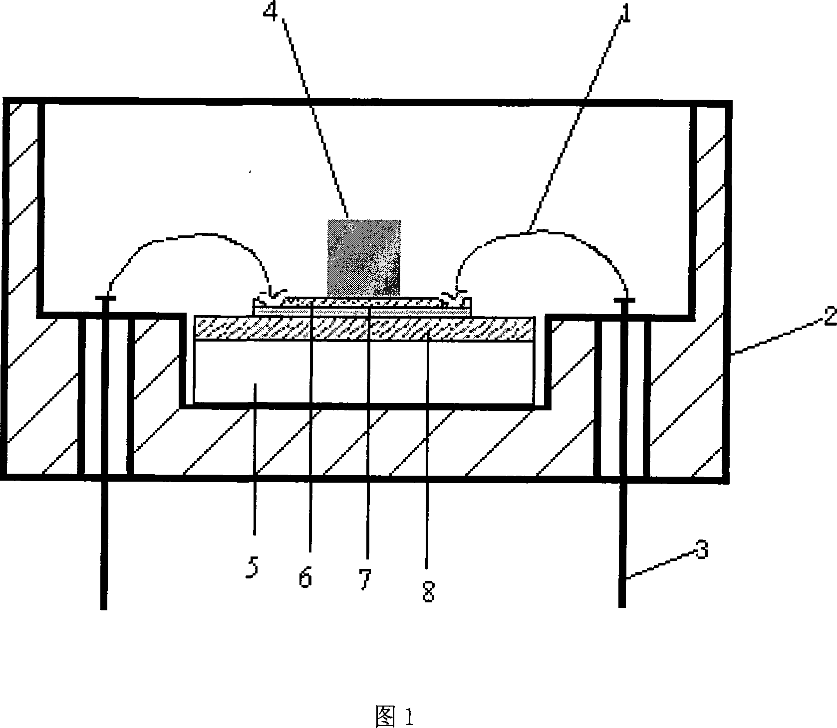
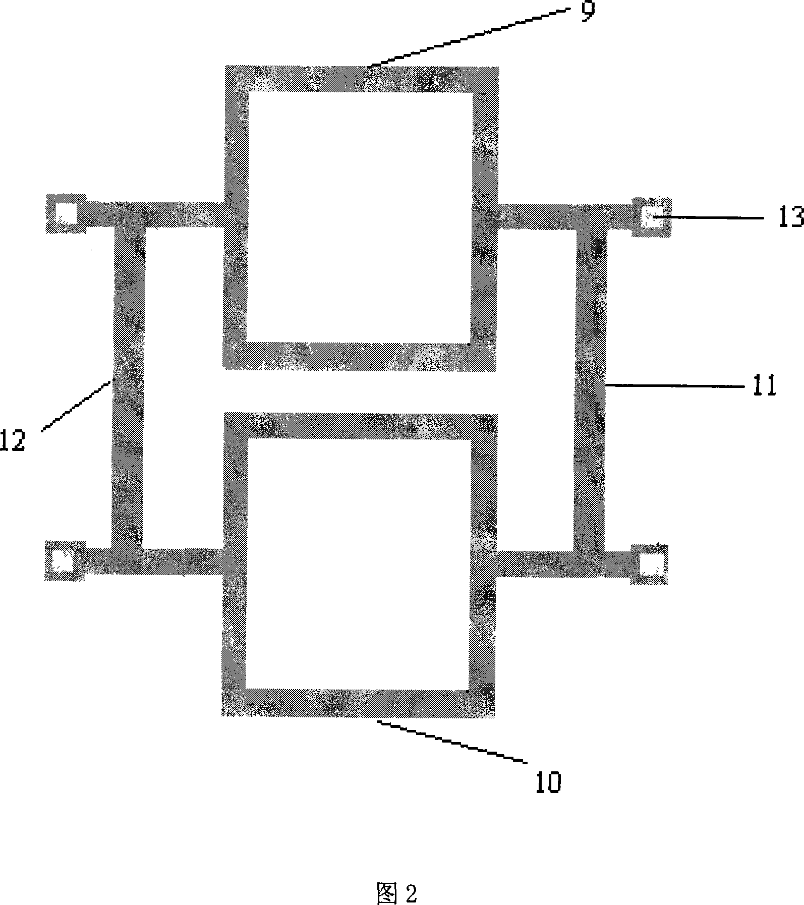
Image

Examples
Embodiment 1
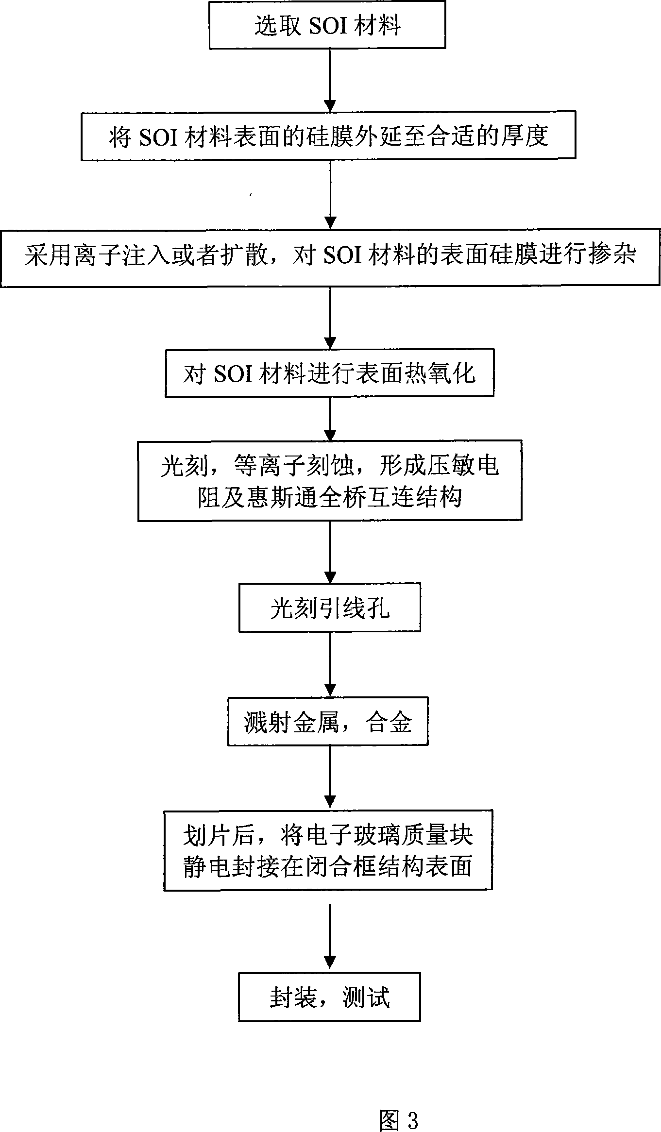
[0045] Fabrication of pressure sensor using 4-inch surface silicon film as P-type SOI wafer
[0046] (1) Epitaxy to make the thickness of the silicon film on the surface reach 2μm;
[0047] (2) The silicon film on the surface of the SOI material is doped with boron by the diffusion process, the pre-deposition temperature is 980°C; the redistribution temperature is 1100°C, the time is 60 minutes, and the surface doping concentration of the piezoresistor is 5×10 19 cm -3 ;
[0048] (3) Thermal oxidation surface silicon film growth SiO 2 , the temperature is 1100°C, the time is 20 minutes, and the thickness is 320nm;
[0049] (4) Use photolithography to remove the thermal oxidation grown SiO in areas other than the closed frame and strip resistors 2 layer, forming a closed frame structure varistor, a strip varistor and a Wheatstone full-bridge interconnection structure;
[0050](5) Plasma etching technology is used to etch the doped silicon thin film layer except the closed ...
Embodiment 2
[0059] Fabrication of pressure sensors using p-type SOI wafers with a 5-inch surface silicon film
[0060] (1) Epitaxy to make the thickness of the silicon film on the surface reach 5 μm;
[0061] (2) The silicon film on the surface of the SOI material is doped with boron by diffusion process, the pre-deposition temperature is 960°C; the redistribution temperature is 1200°C, the time is 90 minutes, and the resistance doping concentration is 6×10 19 cm -3 ;
[0062] (3) Thermal oxidation surface silicon film growth SiO 2 layer, the temperature is 1100°C, the time is 10 minutes, and the thickness is 300nm;
[0063] (4) Use photolithography to remove the thermal oxidation grown SiO in areas other than the closed frame and strip resistors 2 layer, forming a closed frame structure varistor, a strip varistor and a Wheatstone full-bridge interconnection structure;
[0064] (5) Plasma etching technology is used to etch the doped silicon thin film layer except the closed frame and...
Embodiment 3
[0070] Fabrication of pressure sensor using 4-inch surface silicon film as P-type SOI wafer
[0071] (1) Epitaxy to make the thickness of the silicon film on the surface reach 4 μm;
[0072] (2) The silicon film on the surface of the SOI material is doped with boron by the diffusion process, the pre-deposition temperature is 960°C; the redistribution temperature is 1100°C, the time is 50 minutes, and the resistance doping concentration is 3×10 19 cm -3 ;
[0073] (3) Thermal oxidation surface silicon film growth SiO 2 layer, the temperature is 1200°C, the time is 30 minutes, and the thickness is 350nm;
[0074] (4) Use photolithography to remove the thermal oxidation grown SiO in areas other than the closed frame and strip resistors 2 layer, forming a closed frame structure varistor, a strip varistor and a Wheatstone full-bridge interconnection structure;
[0075] (5) Plasma etching technology is used to etch the doped silicon thin film layer except the closed frame and s...
PUM
| Property | Measurement | Unit |
|---|---|---|
| Thickness | aaaaa | aaaaa |
| Thickness | aaaaa | aaaaa |
| Thickness | aaaaa | aaaaa |
Abstract
Description
Claims
Application Information