Method of manufacturing magnetic micro-structure

A fabrication method and microstructure technology, applied in the directions of microstructure technology, microstructure device, manufacturing microstructure device, etc., can solve the problems of magnetic microstructure height limitation, complicated process, only below 50μm, etc., to reduce the requirements and Relying on, avoiding height restrictions, and making the process simple and fast

Inactive Publication Date: 2008-01-23
SHANGHAI INST OF MICROSYSTEM & INFORMATION TECH CHINESE ACAD OF SCI
View PDF0 Cites 29 Cited by
  • Summary
  • Abstract
  • Description
  • Claims
  • Application Information

AI Technical Summary

Problems solved by technology

[0006] Existing research proposes to use electroplating or electrodeposition methods to make some magnetic microstructures in the fluid chip, and generate a local high-gradient magnetic field inside the chip to capture the magnetic beads through the polarization of an external magnetic field, although this method can Avoid the gradual thermal effect of the planar electric coil, but it still needs to use the electroplating process, the process is complicated, and the height of the magnetic microstructure produced is limited by the electroplating process, and generally it can only be below 50 μm, which limits the magnetic microstructure in microflow. Further applications and developments in control chips

Method used


Image

  • Method of manufacturing magnetic micro-structure
  • Method of manufacturing magnetic micro-structure

Examples


Embodiment 1

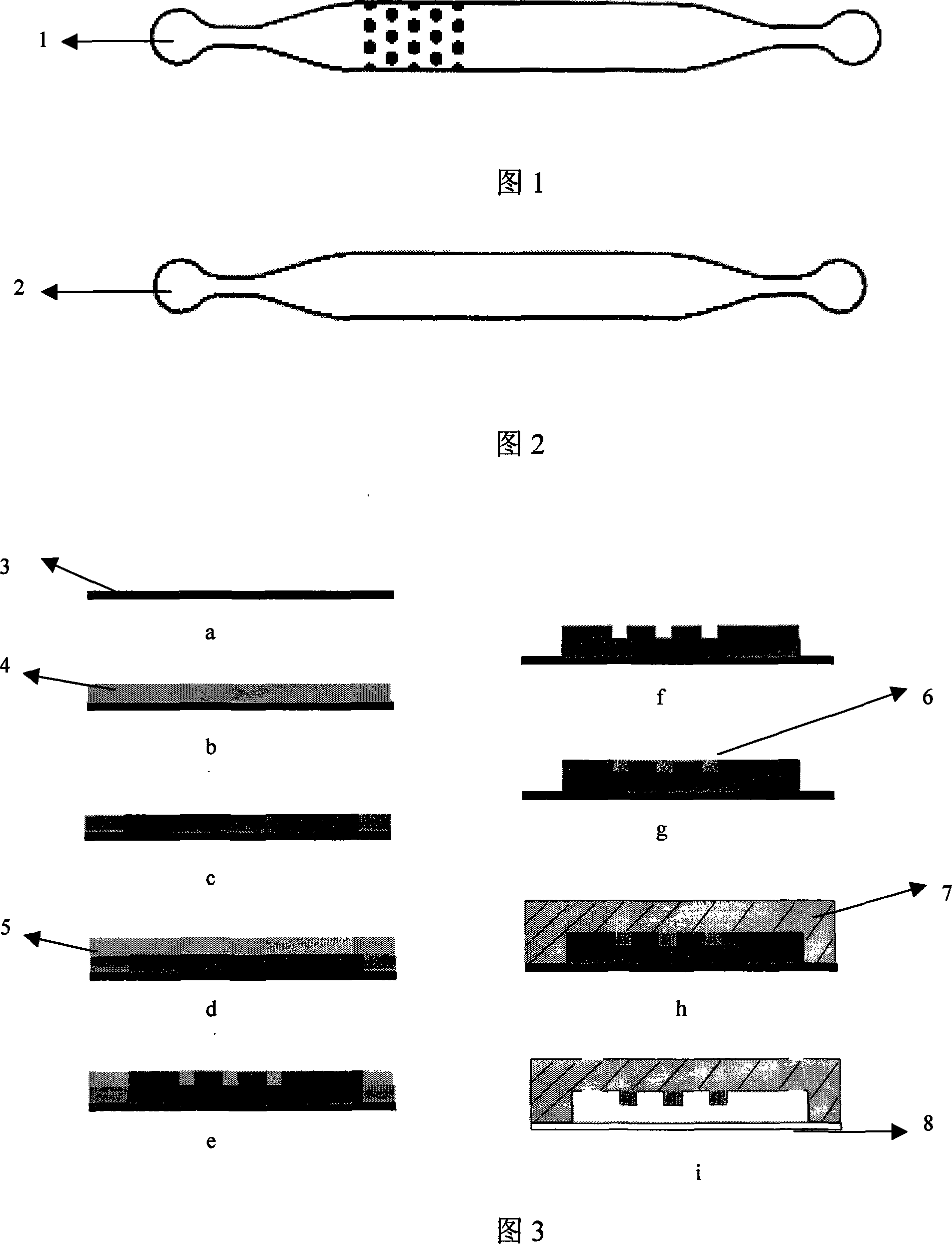
[0059] The following describes in conjunction with Figure 3, taking the fabrication of a magnetic microcolumn array with a height of 100 μm in a PDMS chip as an example, and details the specific process flow of this method for fabricating a microfluidic chip. The chip can be used for sample enrichment, DNA purification, protein capture, online enzyme reaction, etc. The specific process is shown in Figure 3, including the following nine steps:

[0060] (a) The standard RCA cleaning process is used, that is, the Piranha washing solution (H 2 SO 4 :H 2 o 2 ), RCA1 (NH 3 ·H 2 O:H 2 o 2 :H 2 O), RCA2 (concentrated hydrochloric acid: H 2 o 2 :H 2 O) Strictly clean the surface of the silicon wafer 3, and then dry it strictly in an oven or a hot plate after blowing it dry with nitrogen gas [Fig. 3 (a)];

[0061] (b) Spin-coat a layer of SU-8 2050 photoresist (provided by MicroChem) 4 on the front of the silicon wafer, and pre-baked and cured [Figure 3(b)];

[0062] (c) Ali...

Embodiment 2

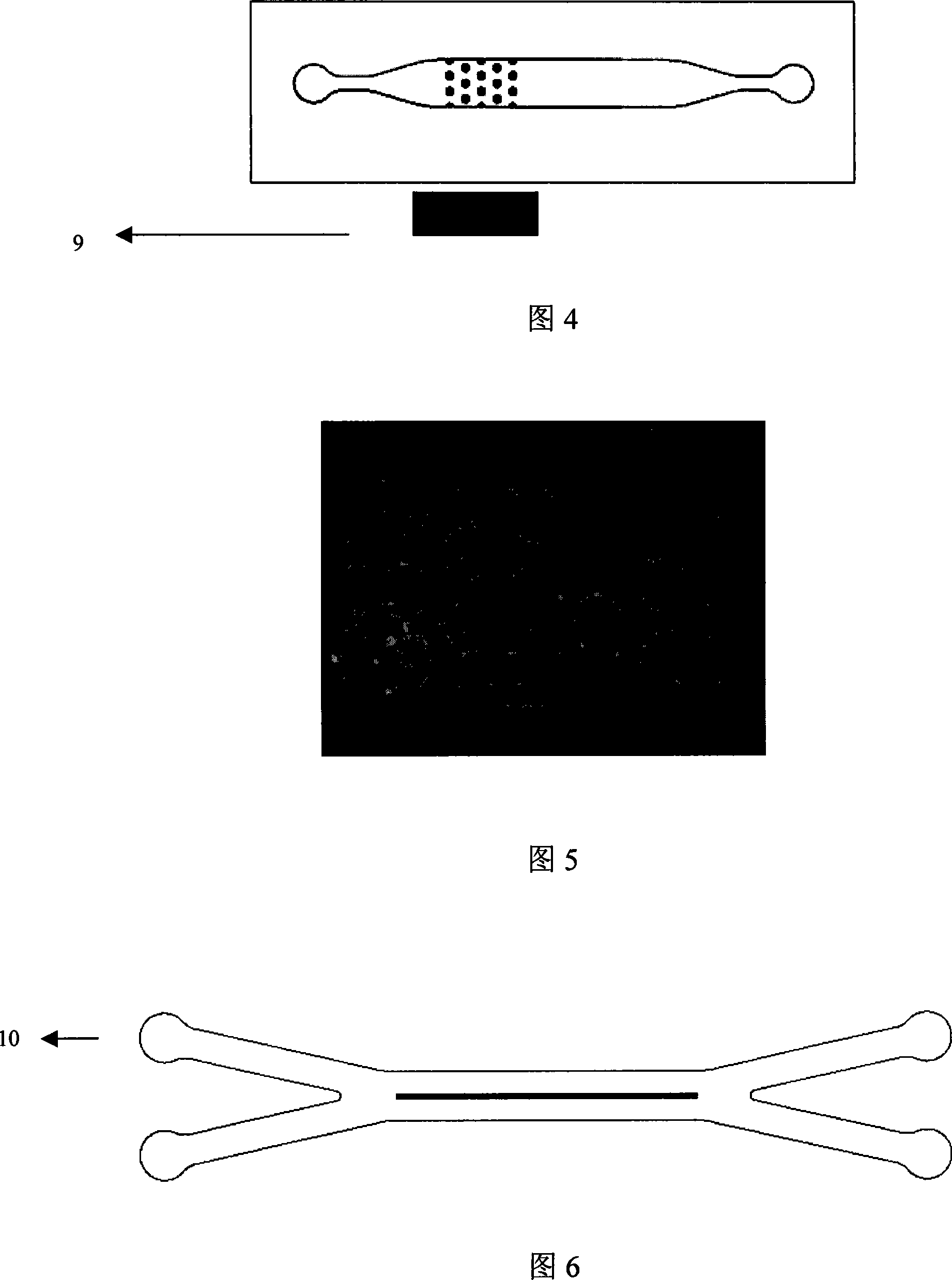
[0072] The basic processing technology of the cell screening chip with a magnetic micro-strip structure ( FIG. 6 ) is the same as that of the magnetic micro-column array chip in Example 1.

[0073] This embodiment applies:

[0074] Mark the magnetic beads on the target cells, pass the sample solution into the microchannel, place a magnet on one side of the chip, wait until the cells marked with magnetic beads are basically adsorbed around the microline, then remove the magnetic field, continue to pass in the solution, and mark with magnetic beads The cells of the beads and the cells of the unlabeled magnetic beads will flow out from the blocked outlet respectively, and the cell screening is completed.


PUM

PropertyMeasurementUnit
heightaaaaaaaaaa

Abstract

The invention relates to a fabrication method of the magnetic microstructure, which is characterized in that the invention comprises the fabrication of multilayer mould and the fabrication of the magnetic microstructure. The former is that the standard RCA cleaning process is used to clean silicon chips; multi layers of SU-8 photoresist are coated by rotating on the silicon chip surfaces and the multi layers of SU-8 mould are gotten after prebaking, photoetching, post baking and developing, and then the invention forms the magnetic microcolumn structure in the chip while molding dying the PDMS chip through directly filling the magnetic powders in the multilayer mould. Adopting the provided fabrication method can dispense with the electroplating process and fabricate the magnetic microstructure in the microfluid chip rapidly. The microstructure height is fabricated between micrometers less than ten and hundred of micrometers, which is determined by the photoresist layers of the rotating coating SU-8 and the magnetic microstructure is any one of the microcolumn, microline, microring or microcoil.

Description

technical field [0001] The invention relates to a manufacturing method of a magnetic microstructure (such as a microcolumn, a microline, a microring, a microcoil, etc.), and belongs to the technical field of microfabrication. Background technique [0002] Immunomagnetic bead technology is a new type of material that emerged in the 1970s. Magnetic beads are microspheres coated with magnetic iron oxide, and the magnetic microspheres are coated with monoclonal antibodies, which can specifically bind to target substances containing corresponding antigens to form new complexes. The complex has magnetic responsiveness different from other components in the magnetic field, and under the action of the magnetic force, the complex moves mechanically, so as to achieve the purpose of separating the antigen. This process of separating from other components is called Immuno-Magnetic Separation. [0003] When the size of magnetic beads reaches the nanometer level, the small size effect o...

Claims


Application Information

Patent Timeline
Patent Type & Authority Applications(China)
IPC IPC(8): B81C1/00B81B1/00H01F41/00
Inventor 封松林王聿佶金庆辉程建功赵建龙
Owner SHANGHAI INST OF MICROSYSTEM & INFORMATION TECH CHINESE ACAD OF SCI
Why Eureka
Try Eureka