Method for building sub-micron or nano-scale formwork by micrometre scale formwork
A sub-micron and nano-scale technology, which is applied in the direction of photolithography, optics, and optomechanical equipment on the patterned surface, can solve the problems of small size and high production cost of sub-micron-sized structures, and achieve short time consumption and low production cost. Inexpensive, high-resolution effects
- Summary
- Abstract
- Description
- Claims
- Application Information
AI Technical Summary
Problems solved by technology
Method used
Image

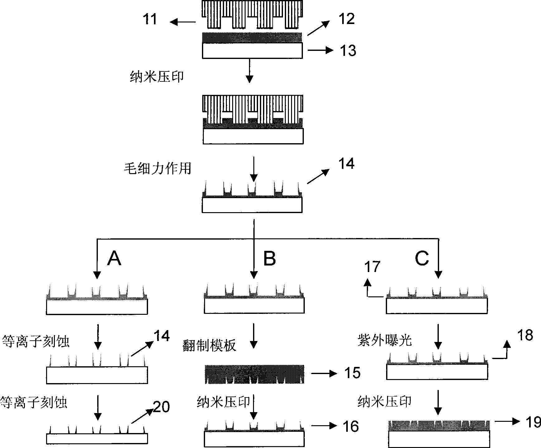
Examples
Embodiment 1
[0048] A PMMA film (sigma-aldrich, weight average molecular weight Mw=96kDa) was prepared by spin-coating on a single crystal silicon substrate ([n type, (100)] or [p type, (100)]), and the thickness of the film was 120nm.
[0049] Fluorosilylating reagent (Heptadecafluoro-1, 1.2, 2-tetrahydradecyl) triethoxysilane, C 16 h 19 f 17 o 3 Si, ABCR GmbH&Co.KG) was assembled onto the surface of the template (5 μl of fluorosilylating reagent was added dropwise, the pressure was maintained at 0.012±0.002Mpa, and the deposition was carried out for 30 minutes). The purpose of this deposition was to treat the surface of the template into a surface with low surface energy, Prevent the polymer from sticking to the template and damaging the template when other polymers are imprinted with this template.
[0050] The rigid template is single crystal silicon, which is prepared by plasma etching. It has a striped structure, the height of the protrusions is 600nm, the structural period is 4μm...
Embodiment 2
[0054] Take the polymer double ridge structure obtained in Example 1, etch the polymer with plasma etching, the polymer and the polymer double ridge layer are generally removed to the same thickness, and the remaining polymer barrier layer on the silicon substrate is etched removed, exposing the underlying silicon substrate. The etching conditions are: O 2 The flow rate is 0.02L / min, the pressure of the cavity is 10mTorr, the etching power is 50W, and the etching time is 3min.
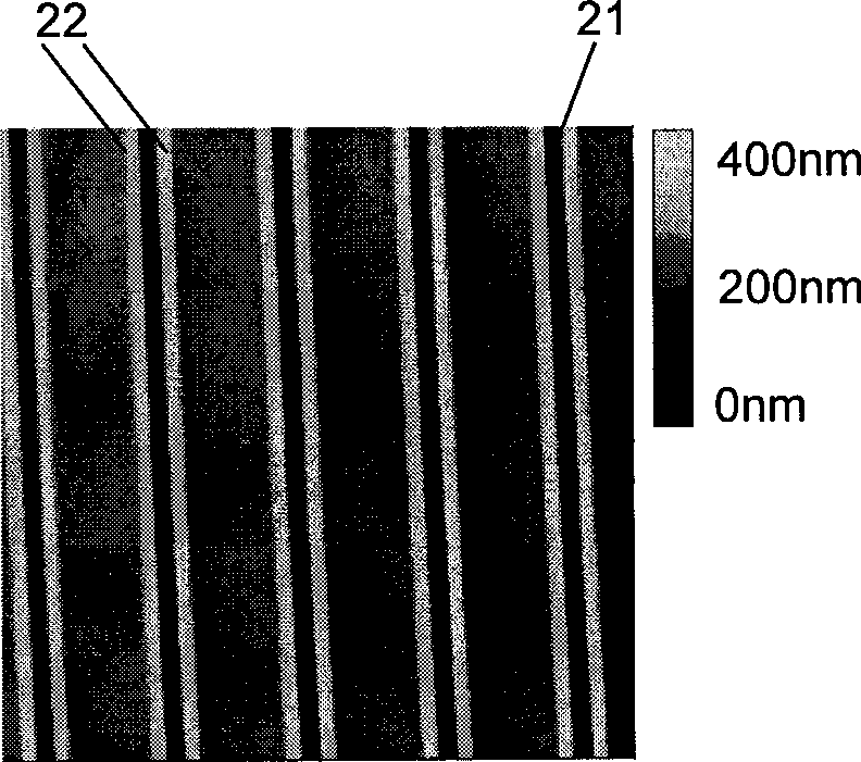
[0055] The etched double-ridge structure was observed with the Tapping mode of the atomic force microscope, such as image 3 As shown, the scanning range is 20 μm × 20 μm. The dark part (dark color part) in the figure is the exposed silicon substrate, and the bright part (light color part) is the polymer double ridge, that is, the attached figure 1 The part shown in the serial number 14. From the analysis results, the height of the double ridges of the remaining polymer is 170nm, the width of the r...
Embodiment 3
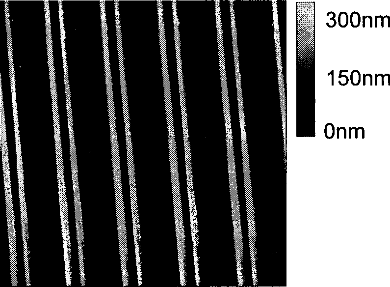
[0057] With the remaining polymer double ridge structure in Example 2 as a barrier layer, continue to use the plasma etching technology to utilize SF 6 and O 2 The monocrystalline silicon substrate is etched. The etching conditions are: O 2 The flow rate is 0.01L / min, SF 6The flow rate is 0.05L / min, the chamber pressure is 10mTorr, the etching power is 30W, and the etching time is 2min to remove the polymer double ridge and part of the silicon substrate. After etching, use acetone, chloroform, absolute ethanol, and deionized water to ultrasonically clean for 3 minutes in sequence, and use the atomic force microscope Tapping mode to observe the double-ridge structure of the etched silicon substrate, as shown in Fig. Figure 4 As shown, the scanning range is 20μm×20μm. The dark part (dark color part) in the figure is the place where the silicon substrate is relatively low, and the bright part (light color part) is the place where the silicon substrate is relatively high. fig...
PUM
| Property | Measurement | Unit |
|---|---|---|
| Thickness | aaaaa | aaaaa |
| Height | aaaaa | aaaaa |
| Ridge width | aaaaa | aaaaa |
Abstract
Description
Claims
Application Information
 - Generate Ideas
- Intellectual Property
- Life Sciences
- Materials
- Tech Scout
- Unparalleled Data Quality
- Higher Quality Content
- 60% Fewer Hallucinations
Browse by: Latest US Patents, China's latest patents, Technical Efficacy Thesaurus, Application Domain, Technology Topic, Popular Technical Reports.
© 2025 PatSnap. All rights reserved.Legal|Privacy policy|Modern Slavery Act Transparency Statement|Sitemap|About US| Contact US: help@patsnap.com