

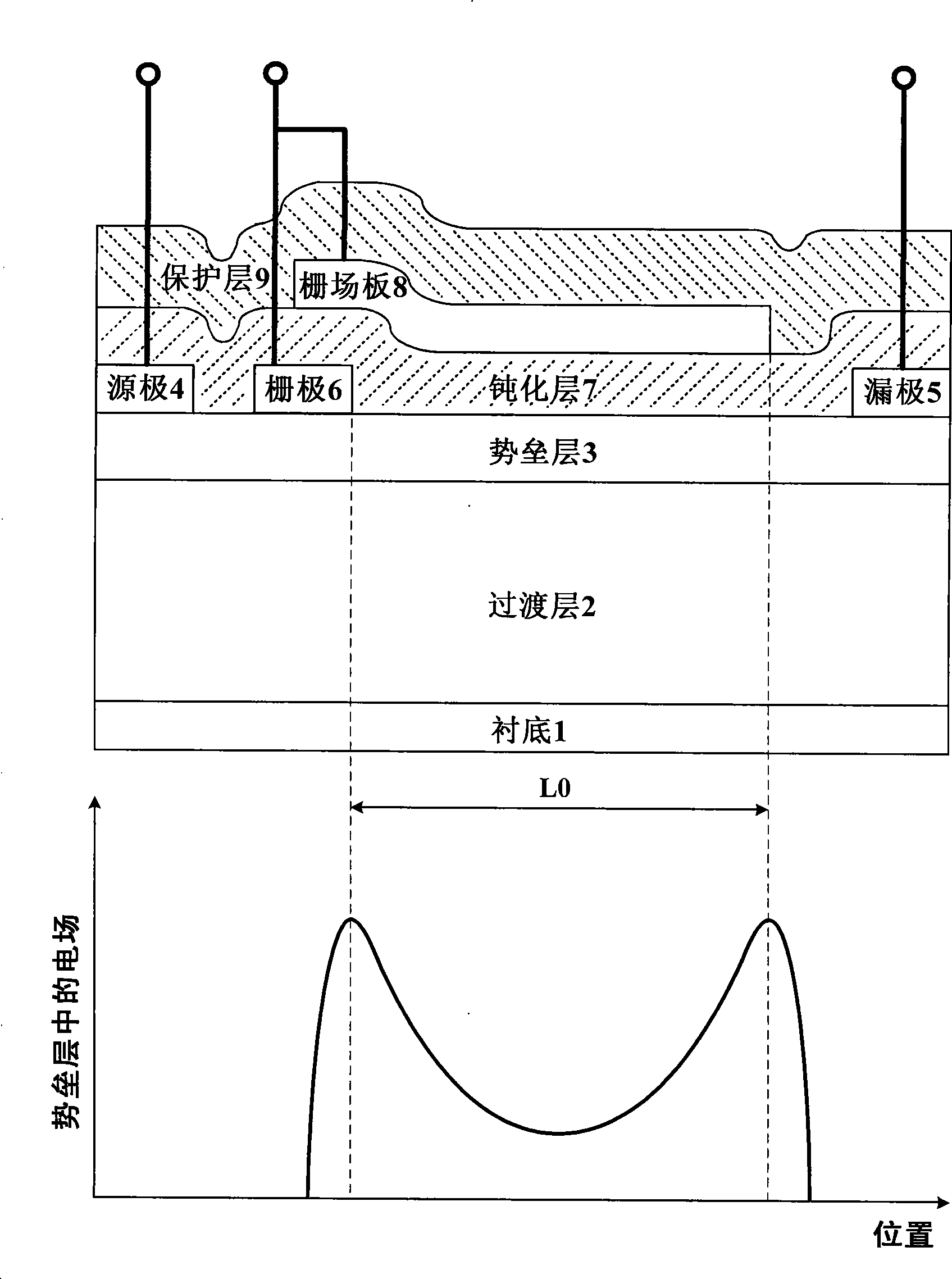
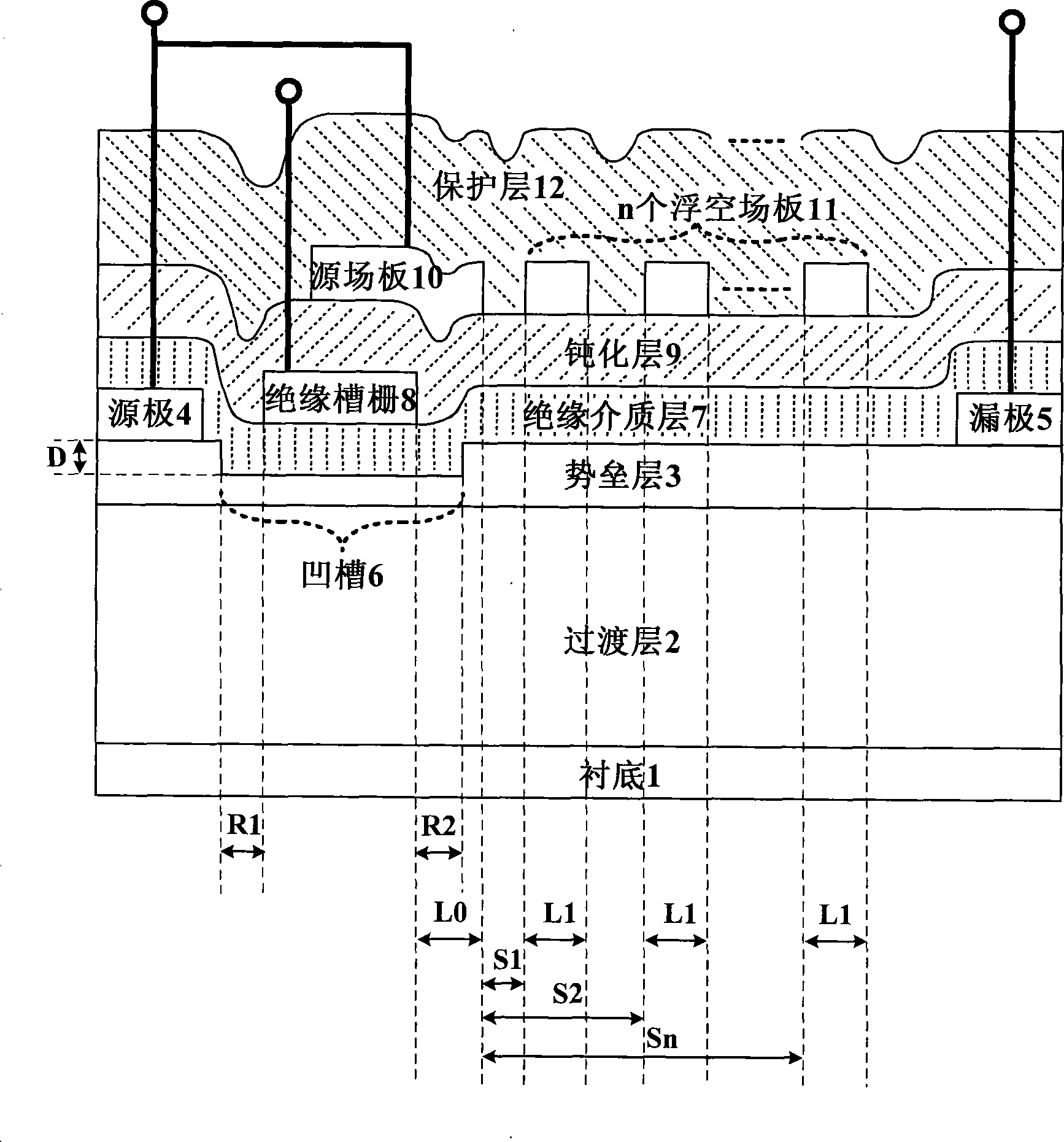
Heterojunction field effect transistor for groove insulated gate type multiple source field plate
A heterojunction field effect, insulated gate type technology, applied in the field of microelectronics, can solve the problems of reducing the yield of the device, complicated manufacturing process, tedious process debugging, etc., to reduce leakage current, reduce electric field lines, and reduce electric field. Effect
- Summary
- Abstract
- Description
- Claims
- Application Information
AI Technical Summary
Problems solved by technology
Method used
Image

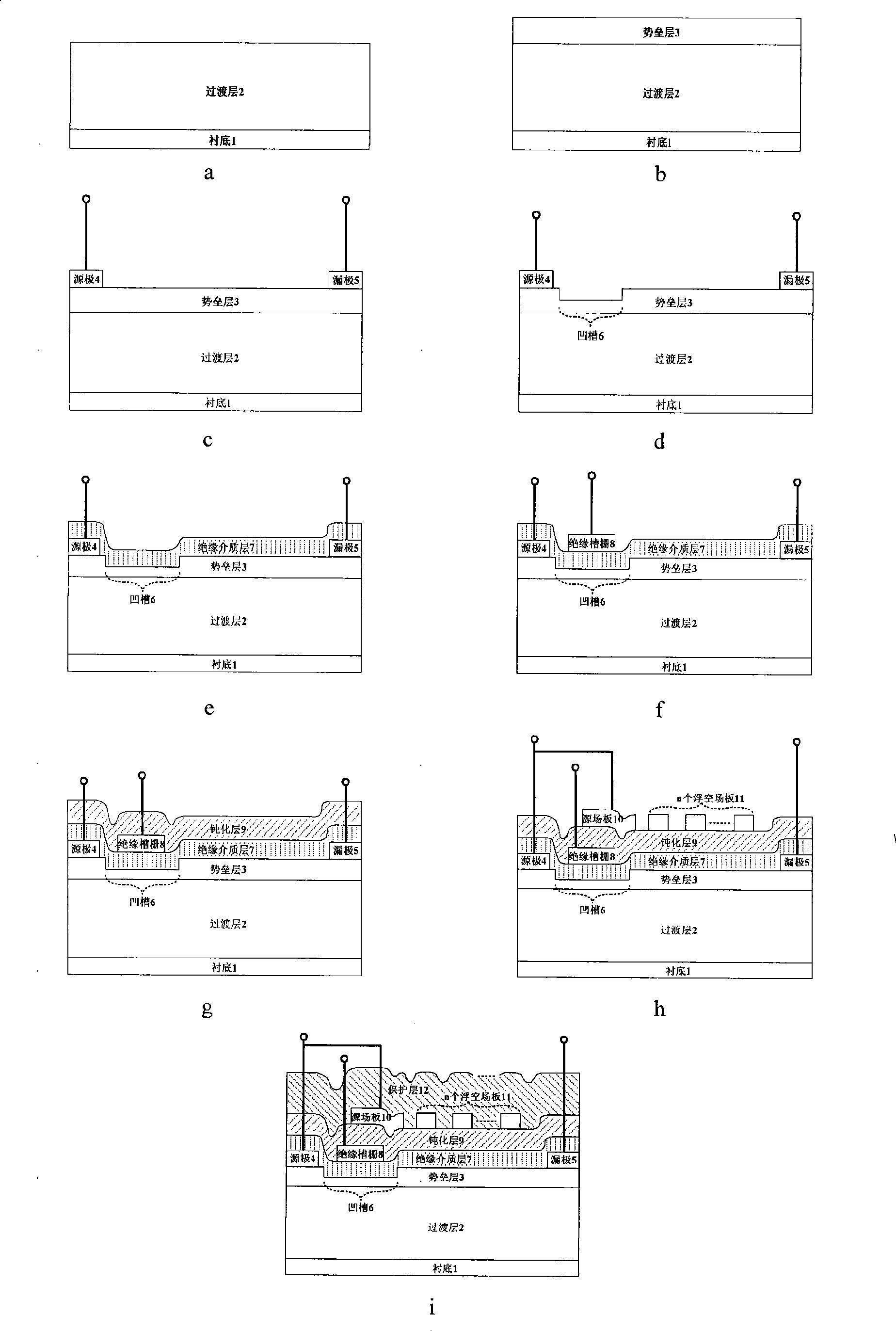
Examples
Embodiment 1
[0060] The production substrate is sapphire, and the insulating dielectric layer is SiO 2 , the passivation layer is SiN, the protective layer is SiN, the source field plate and each floating field plate is a heterojunction field effect transistor with a composite source field plate composed of Ti / Au metal, and the process is:
[0061] 1. Using metal organic chemical vapor deposition technology to epitaxially undoped transition layer 2 with a thickness of 1 μm on the sapphire substrate 1, the transition layer is composed of AlN material with a thickness of 26 nm and GaN material with a thickness of 0.974 μm from bottom to top constitute. The process conditions used for the epitaxial lower layer AlN material are: temperature 575°C, pressure 82 Torr, hydrogen gas flow rate 4400 sccm, ammonia gas flow rate 4400 sccm, aluminum source flow rate 26 μmol / min; the process conditions for the epitaxial upper layer GaN material are: temperature 1000°C, the pressure is 82 Torr, the flow ...
Embodiment 2
[0071] The production substrate is silicon carbide, the insulating dielectric layer is SiN, and the passivation layer is SiO 2 , the protective layer is SiO 2 , the source field plate and each floating field plate is a heterojunction field effect transistor with a composite source field plate of Ni / Au metal combination, and the process is:
[0072] 1. An undoped transition layer 2 with a thickness of 2.6 μm is epitaxially formed on a silicon carbide substrate 1 by metal-organic chemical vapor deposition technology. Made of GaN material. The process conditions used for the epitaxial lower layer AlN material are: temperature 1040°C, pressure 85 Torr, hydrogen gas flow rate 5000 sccm, ammonia gas flow rate 5000 sccm, aluminum source flow rate 16 μmol / min; the process conditions for the epitaxial upper layer GaN material are: temperature 1040°C, the pressure is 85 Torr, the flow rate of hydrogen gas is 5000 sccm, the flow rate of ammonia gas is 5000 sccm, and the flow rate of ga...
Embodiment 3
[0082] The production substrate is silicon, and the insulating dielectric layer is Al 2 o 3 , the passivation layer is SiN, the protective layer is SiN, the source field plate and each floating field plate is a heterojunction field effect transistor with a composite source field plate composed of Pt / Au metal, and the process is:
[0083] 1. Using metal organic chemical vapor deposition technology to epitaxially undoped transition layer 2 with a thickness of 5 μm on the silicon substrate 1, the transition layer is composed of AlN material with a thickness of 135 nm and GaN material with a thickness of 4.865 μm from bottom to top constitute. The process conditions used for the epitaxial lower layer AlN material are: temperature 880°C, pressure 90 Torr, hydrogen gas flow rate 5100 sccm, ammonia gas flow rate 5100 sccm, aluminum source flow rate 41 μmol / min; the process conditions for the epitaxial upper layer GaN material are: temperature 1070°C, pressure 90 Torr, hydrogen gas ...
PUM
 Abstract
Description
Claims
Application Information