

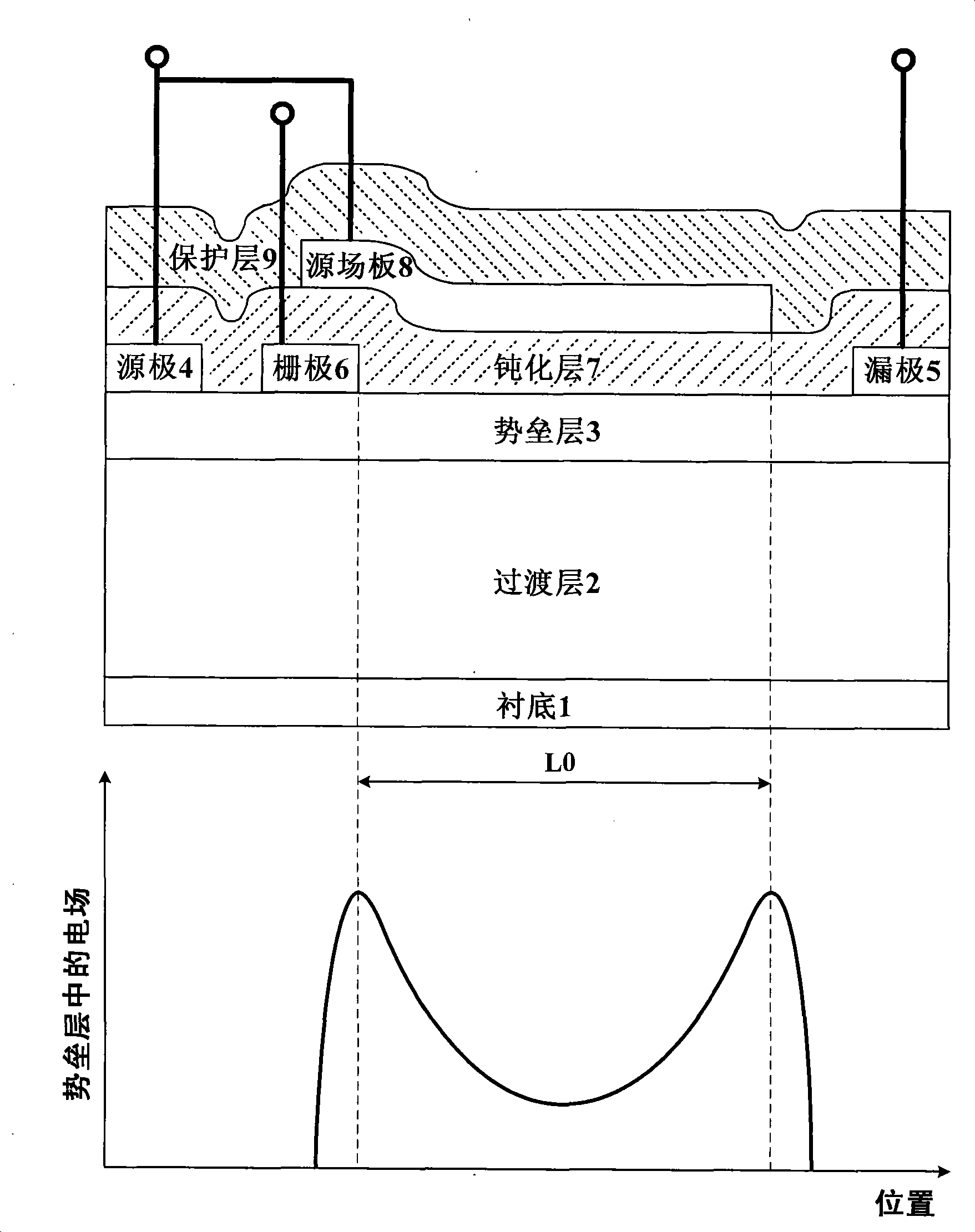
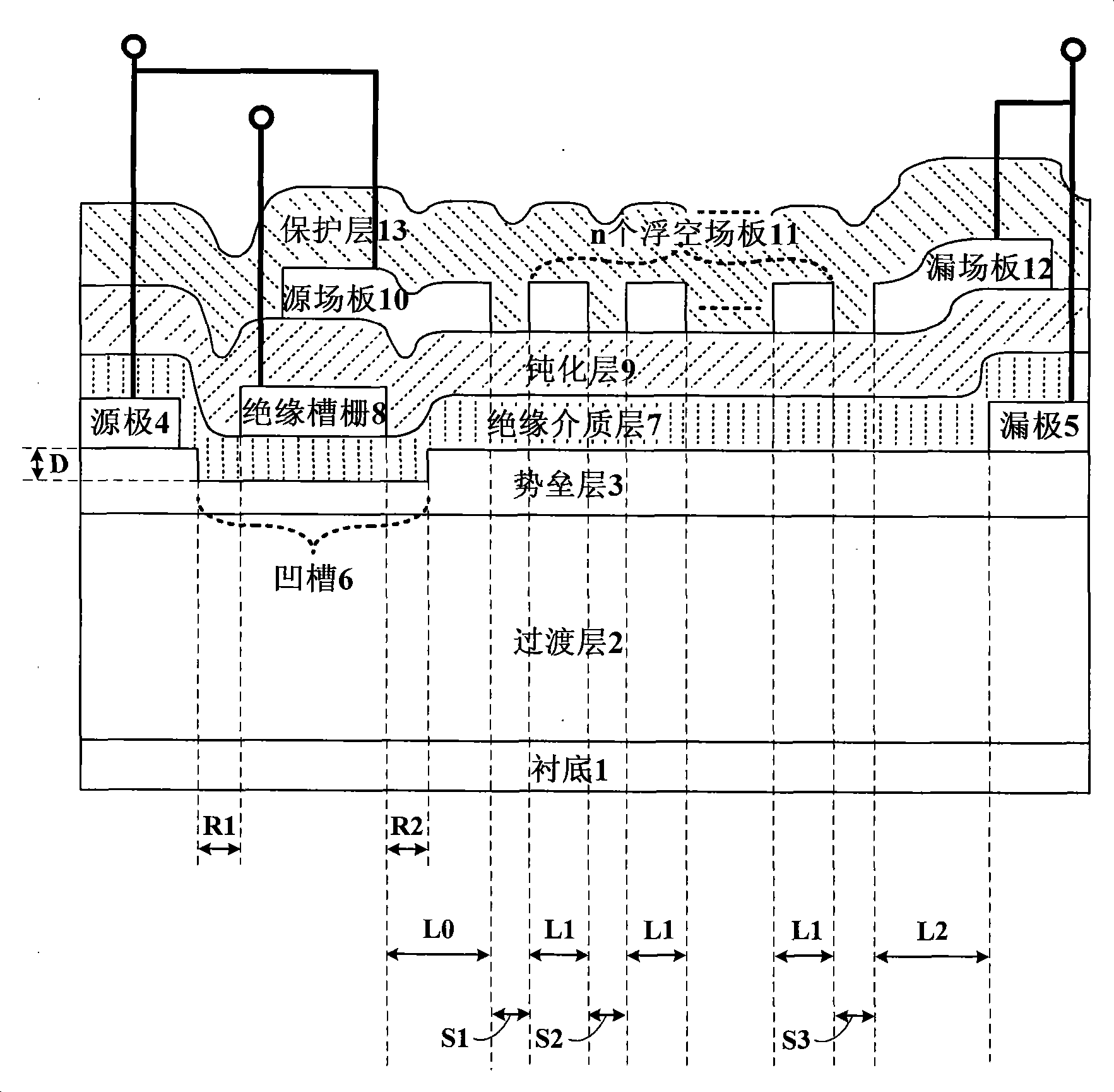
Groove insulated gate type source-leakage composite field plate transistor with high electron mobility
A technology with high electron mobility and insulated gate type, which is applied in the field of microelectronics, can solve the problems of reducing device yield, increasing device difficulty, and complicated manufacturing process, so as to improve breakdown voltage, reduce gate leakage current, and enhance reliability effect
- Summary
- Abstract
- Description
- Claims
- Application Information
AI Technical Summary
Problems solved by technology
Method used
Image

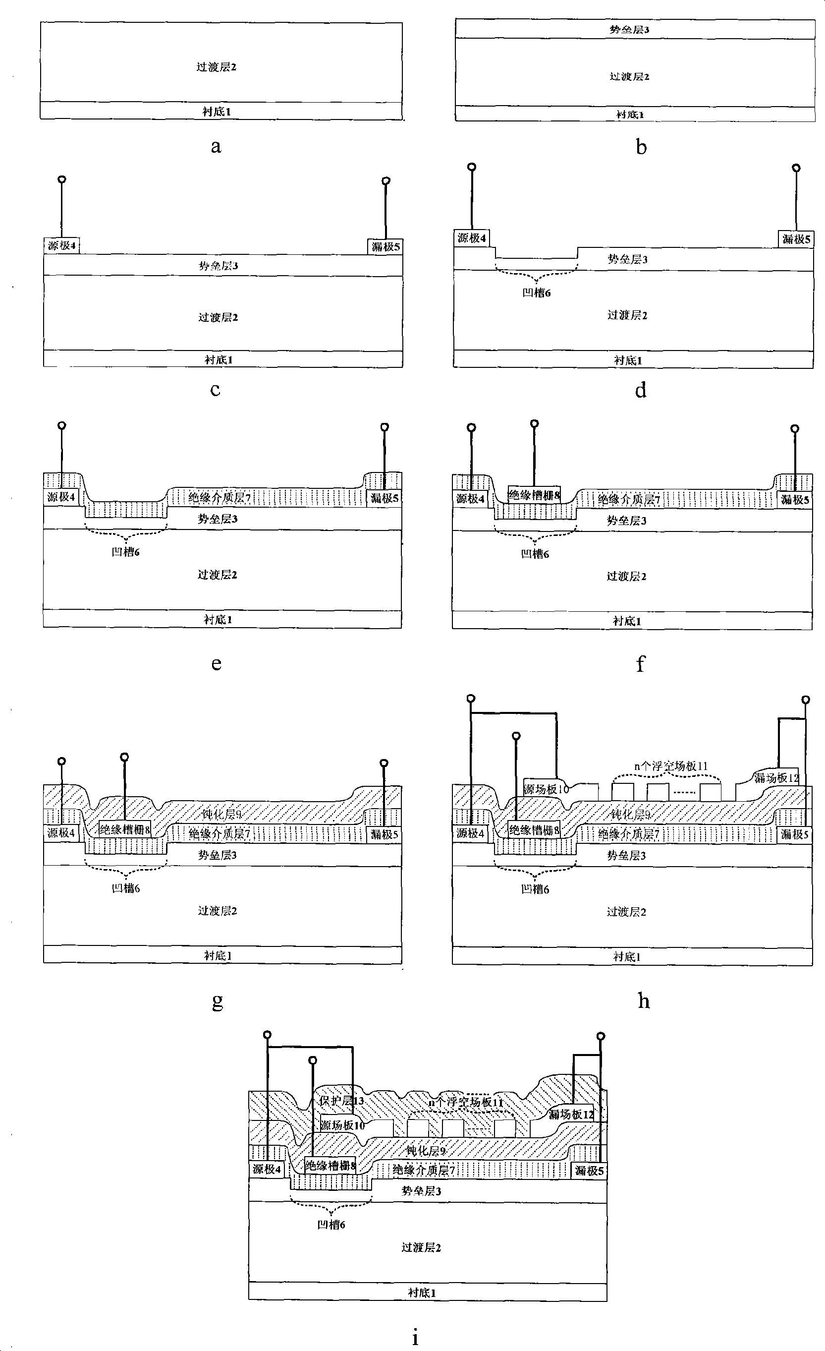
Examples
Embodiment 1
[0061] The production substrate is sapphire, and the insulating dielectric layer is SiO 2 , the passivation layer is SiN, the protective layer is SiN, the source field plate, the drain field plate and each floating field plate are Ti / Au metal combination source-drain compound field plate high electron mobility transistor, and the process is:
[0062] 1. Using metal organic chemical vapor deposition technology to epitaxially undoped transition layer 2 with a thickness of 1 μm on the sapphire substrate 1, the transition layer is composed of AlN material with a thickness of 33 nm and GaN material with a thickness of 0.967 μm from bottom to top constitute. The process conditions used for the epitaxial lower layer AlN material are: temperature 590°C, pressure 160 Torr, hydrogen gas flow rate 4700 sccm, ammonia gas flow rate 4700 sccm, aluminum source flow rate 35 μmol / min; the process conditions for the epitaxial upper layer GaN material are: temperature 1050°C, pressure 160 Torr,...
Embodiment 2
[0072] The production substrate is silicon carbide, the insulating dielectric layer is SiN, and the passivation layer is SiO 2 , the protective layer is SiO 2 , the source field plate, the drain field plate and each floating field plate are Ni / Au metal combination source-drain compound field plate high electron mobility transistor, the process is:
[0073] 1. An undoped transition layer 2 with a thickness of 2.1 μm is epitaxially formed on a silicon carbide substrate 1 by metal-organic chemical vapor deposition technology. Made of GaN material. The process conditions used for the epitaxial lower layer AlN material are: temperature 1020°C, pressure 165 Torr, hydrogen gas flow rate 4800 sccm, ammonia gas flow rate 4800 sccm, aluminum source flow rate 12 μmol / min; the process conditions for the epitaxial upper layer GaN material are: temperature 1020°C, pressure 165 Torr, hydrogen flow rate 4800 sccm, ammonia gas flow rate 4800 sccm, gallium source flow rate 160 μmol / min.
[0...
Embodiment 3
[0083] The production substrate is silicon, and the insulating dielectric layer is Al 2 o 3 , the passivation layer is SiN, the protective layer is SiN, the source field plate, the drain field plate and each floating field plate are Pt / Au metal combined source-drain compound field plate high electron mobility transistors, and the process is:
[0084] 1. Using metal organic chemical vapor deposition technology to epitaxially undoped transition layer 2 with a thickness of 5 μm on the silicon substrate 1, the transition layer is composed of AlN material with a thickness of 125 nm and GaN material with a thickness of 4.875 μm from bottom to top constitute. The process conditions used for the epitaxial lower layer AlN material are: temperature 860°C, pressure 170 Torr, hydrogen gas flow rate 4900 sccm, ammonia gas flow rate 4900 sccm, aluminum source flow rate 35 μmol / min; the process conditions for the epitaxial upper layer GaN material are: temperature 1050°C, pressure 170 Torr...
PUM
| Property | Measurement | Unit |
|---|---|---|
| Thickness | aaaaa | aaaaa |
| Thickness | aaaaa | aaaaa |
| Thickness | aaaaa | aaaaa |
Abstract
Description
Claims
Application Information