Organic photolectronic device with an updoped gain layer and preparation method thereof

An optoelectronic device, non-doped technology, applied in the direction of electric solid device, semiconductor/solid state device manufacturing, electrical components, etc., can solve problems affecting device performance, reduce device manufacturing cost, and achieve complex implementation, and achieves low manufacturing process requirements. Overcome technical difficulties and the effect of simple device structure

Inactive Publication Date: 2009-10-14
UNIV OF ELECTRONICS SCI & TECH OF CHINA
View PDF4 Cites 19 Cited by
  • Summary
  • Abstract
  • Description
  • Claims
  • Application Information

AI Technical Summary

Problems solved by technology

[0003] In the field of organic electroluminescence (OLED), in order to balance the electrons and holes in the light-emitting layer, it is reported that the light-emitting layer is doped with a compound as an electron-accepting dopant or an electron-donating dopant, see 200680016012.7 ( 2006), this patent mainly doped electron-accepting and electron-donating dopants in the light-emitting layer, and the possible result is that the dopant quenches the excitons generated in the light-emitting layer, especially the doping of alkali metal materials in the light-emitting layer In addition, the process of doping metal materials in organic materials is relatively complicated, which increases the complexity and precision of equipment, and increases the difficulty of device realization and production costs.
[0004] In order to improve the cathode electron injection and balance the electron holes, in order to reduce the potential barrier encountered when injecting electrons from the cathode to the organic compound, some studies have also introduced a metal doped layer at the interface of the cathode layer to improve the electron injection. See 98104283.X (1998), although this patent puts metal doping in the electron transport layer, because the electron transport layer is close to the light-emitting layer, the excitons in the light-emitting layer will also be quenched due to collisions with metal atoms when they diffuse , is not conducive to improving device performance
At the same time, the doping of metal materials in electron transport materials is also a mixture of organic materials and inorganic materials, which is difficult to realize and is not conducive to reducing the cost of device manufacturing.
[0005] In addition, the method of setting a buffer layer doped with alkali metal fluoride or alkaline earth metal fluoride between the electron transport layer and the cathode, see 200510069612.7 (2005) for details, for metal materials and organic materials and mixed preparation will increase the process difficulty of device preparation, At the same time, it may affect the film-forming characteristics of the material, thereby affecting the performance of the device
[0006] In addition, metal or metal salt doping is used to form an electron injection layer at the interface of the electron transport layer to improve electron injection. See 01807496.0 (2003) for details. The effect of this patent is limited to the effective injection of electrons. For electrons in the electron transport layer The contribution to the improvement of mobility is not obvious enough. If electrons cannot recombine with holes to form excitons within the effective lifetime, the accumulation of excess electrons in the electron transport layer will also affect the performance of the device.
[0007] In recent years, although organic optoelectronic technology has made great progress, the current technology still has many bottlenecks in the field of organic optoelectronic devices: making simple structural devices, cost, and efficiency are all important factors affecting the practical use of devices, and Because the electron transfer rate is much lower than the hole transfer rate inside the device, the imbalance between electrons and holes in the transport process seriously affects the formation of excitons, resulting in low device efficiency.

Method used


Image

  • Organic photolectronic device with an updoped gain layer and preparation method thereof
  • Organic photolectronic device with an updoped gain layer and preparation method thereof
  • Organic photolectronic device with an updoped gain layer and preparation method thereof

Examples


Embodiment 1

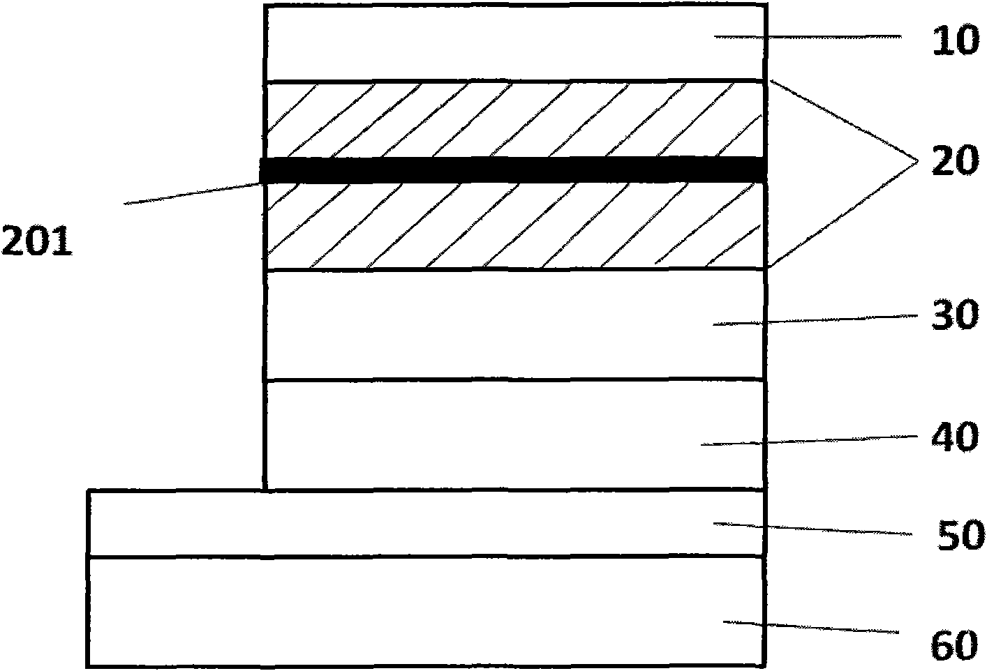
[0097] Such as image 3 As shown, the electron transport layer 20 in the structure of the organic electroluminescent device has a non-doped single-layer metal thin layer 203 .

[0098] The organic electron transport material and luminescent material of the device are Alq 3 , the hole transport material is NPB, the material of the non-doped single-layer metal thin layer 203 is Mg, the cathode layer is Mg:Ag alloy, and the whole device structure A is described as:

[0099] Glass substrate / ITO / NPB(20nm) / Alq 3 (50nm) / Mg(2nm) / Alq 3 (20nm) / Mg:Ag(100nm)

[0100] The preparation method is as follows:

[0101] ①Use acetone solution, deionized water and ethanol solution to ultrasonically clean the conductive substrate ITO glass, and dry it with dry nitrogen after cleaning. Wherein the ITO film on the glass substrate is used as the anode layer of the device, the square resistance of the ITO film is 12Ω / sq, and the film thickness is 180nm.

[0102] ② Move the dried substrate into a ...

Embodiment 2

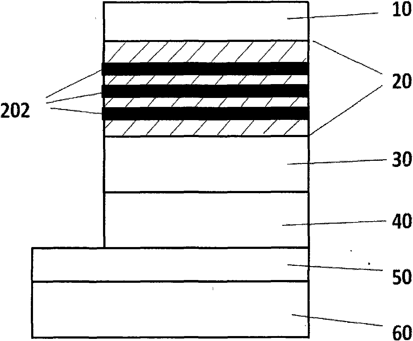
[0115] Such as Figure 6 As shown, the electron transport region 20 in the structure of the organic solar cell device has a non-doped single-layer metal thin layer 204 .

[0116] The organic electron acceptor material of the device is C 60 , the electron donor material is CuPc, the material of the non-doped single-layer metal thin layer 204 is Mg, the metal electrode layer is metal Ag, and the whole device structure is described as:

[0117] Glass substrate / ITO / CuPc(40nm) / C 60 (30nm) / Mg(2nm) / C 60 The preparation process of the (10nm) / Ag(100nm) device is similar to that of Example 1.

Embodiment 3

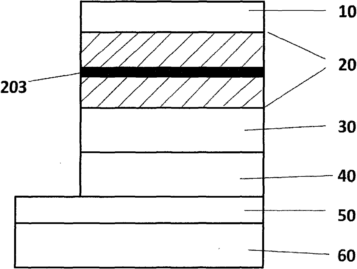
[0119] Such as Figure 7As shown, in the structure of the organic solar cell device, there is a non-doped single-layer metal thin layer 205 in the exciton blocking layer and buffer layer 70 .

[0120] The organic electron acceptor material of the device is C 60 , the electron donor material is CuPc, the exciton blocking layer and buffer layer material is BCP, the material of the non-doped single-layer metal thin layer 205 is Mg, and the cathode layer uses metal Mg. The entire device structure is described as:

[0121] Glass substrate / ITO / CuPc(40nm) / C 60 (40nm) / BCP(20nm) / Mg(2nm) / BCP(10nm) / Ag(100nm)

[0122] The fabrication process of the device is similar to that of Example 1.


PUM


Abstract

The invention discloses an organic photolectronic device with an updoped gain layer, and the structure of the device at least comprises a substrate, a first electrode layer, an organic functional layer, and a second electrode layer; wherein, the organic functional layer comprises an electron transfer layer or an electron acceptor layer, which is characterized in that updoped gain layer with the function of improving electron mobility is equipped in the electron transfer layer or the electron acceptor layer, the thickness of the gain layer is smaller than 5nm and the materials are metal or organic compound with strong electron withdraw groups. The device overcomes the defects of existing technology, improves electron mobility effectively, balances the amount of current carriers such as electrons and cavities inside the device, and has simple structure, low cost and high efficiency.

Description

technical field [0001] The invention relates to the technical field of organic optoelectronics in electronic components, in particular to an organic optoelectronic device with a non-doped gain layer. Background technique [0002] Optoelectronic devices refer to devices capable of photoelectric or electro-optical energy conversion, including photodetectors, solar photovoltaic cells, light-emitting devices and lasers. Such devices generally comprise a pair of electrodes called a cathode and an anode and at least one loading layer sandwiched between the cathode and anode. Depending on the function of the optoelectronic device, one or more loading layers may consist of a material or materials that emit light in response to a voltage applied to the electrodes, or the layer or layers may form a heterojunction that, when exposed to light Photoelectric effect can be produced when irradiated. Many properties of all these functional devices based on organic semiconductor materials a...

Claims


Application Information

Patent Timeline
Patent Type & Authority Applications(China)
IPC IPC(8): H01L51/50H01L51/54H01L51/56
Inventor 蒋亚东于军胜余双江李璐
Owner UNIV OF ELECTRONICS SCI & TECH OF CHINA
Why Eureka
Try Eureka