

Method for manufacturing and integrating multichannel high-sensitive biosensor
A biosensor and integrated method technology, which is applied in the field of silicon nanowire biosensors based on SOI technology, can solve problems such as decreased detection sensitivity, and achieve the effects of reducing false detection rate, high sensitivity, and reducing defective product rate.
- Summary
- Abstract
- Description
- Claims
- Application Information
AI Technical Summary
Problems solved by technology
Method used
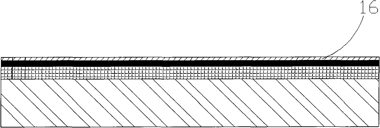
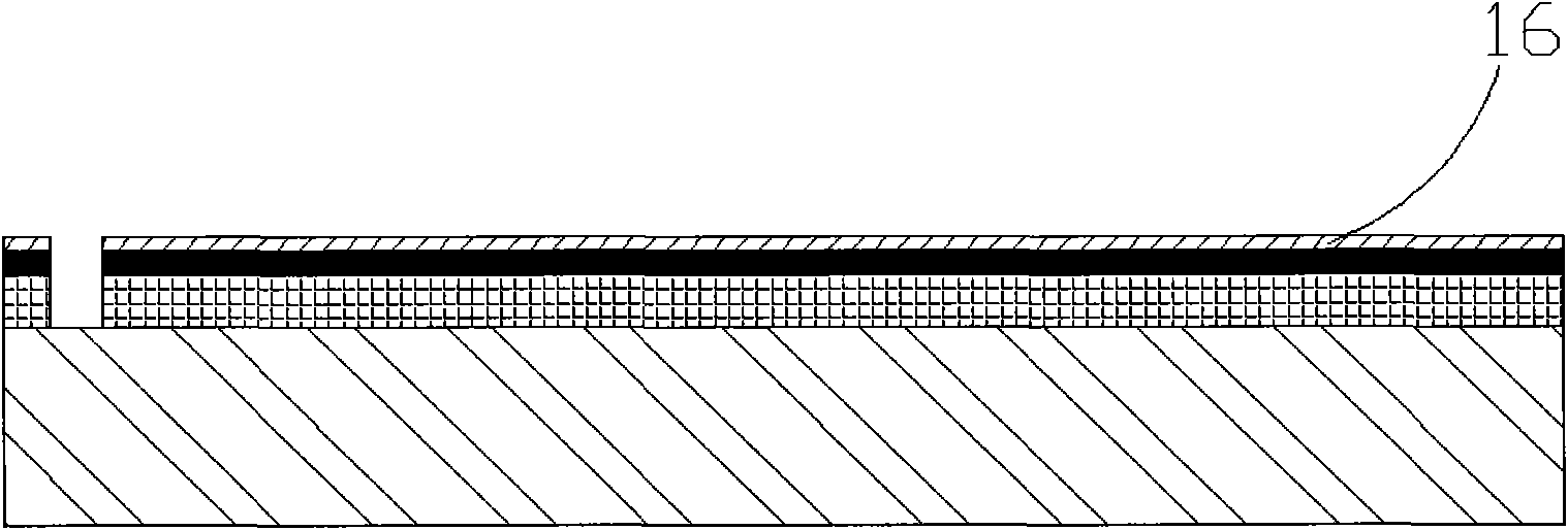
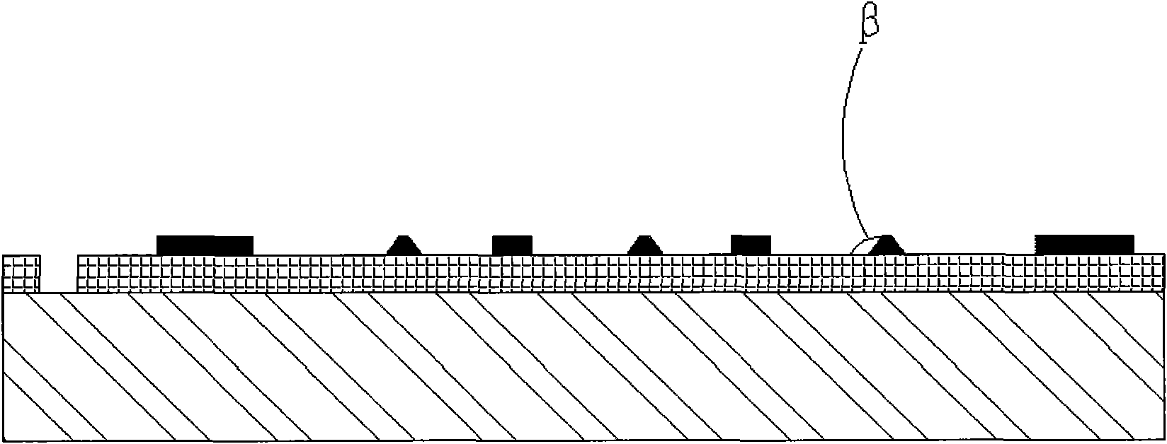
Image

Examples
Embodiment I
[0048] (1) Silicon nanowire FET field effect transistors are manufactured by top-down method based on SOI silicon wafer:
[0049] 1) Silicon wafer cleaning, first boil the silicon wafer with 7:3 concentrated sulfuric acid and hydrogen peroxide at 60 degrees for 15 minutes, then take out the ultrapure water to rinse, then use 1:3:7 ammonia water and hydrogen peroxide solution to boil for 10 minutes, take out the ultrapure water and rinse ; Next, heat in 1:2:8 hydrochloric acid and hydrogen peroxide aqueous solution at 60°C for 10 minutes, take it out, rinse it with ultrapure water, and dry it with nitrogen; corrode it with 5:1 hydrofluoric acid buffer solution for 5 seconds, take it out, and use ultrapure water Rinse and dry with nitrogen gas; dry in a 100-degree oven for 10 minutes; after cleaning, remove the polluting organic matter and metal ions contained on the surface of the silicon wafer;
[0050] 2) To thin the silicon wafer, first oxidize the silicon wafer with wet oxy...
Embodiment II
[0066] (1) Silicon nanowire FET field effect transistors are manufactured by top-down method based on SOI silicon wafer:
[0067] 1) Silicon wafer cleaning, first boil the silicon wafer with 7:3 concentrated sulfuric acid and hydrogen peroxide at 60 degrees for 15 minutes, then take out the ultrapure water to rinse, then use 1:3:7 ammonia water and hydrogen peroxide solution to boil for 10 minutes, take out the ultrapure water and rinse , then heated in 1:2:8 hydrochloric acid and hydrogen peroxide aqueous solution at 60°C for 10 minutes, took it out, rinsed it with ultrapure water, dried it with nitrogen, etched it with 5:1 hydrofluoric acid buffer solution for 5 seconds, took it out, and rinsed it with ultrapure water Rinse, blow dry with nitrogen, and dry in a 100-degree oven for 10 minutes. After cleaning, the contaminated organic matter and metal ions contained on the surface of the silicon wafer are removed;
[0068] 2) Thinning of silicon wafers, first oxidize the silic...
Embodiment III
[0086] (1) Silicon nanowire FET field effect transistors are manufactured by top-down method based on SOI silicon wafer:
[0087] 1) Silicon wafer cleaning, first boil the silicon wafer with 7:3 concentrated sulfuric acid and hydrogen peroxide at 60 degrees for 15 minutes, then take out the ultrapure water to rinse, then use 1:3:7 ammonia water and hydrogen peroxide solution to boil for 10 minutes, take out the ultrapure water and rinse , then heated in 1:2:8 hydrochloric acid and hydrogen peroxide aqueous solution at 60°C for 10 minutes, took it out, rinsed it with ultrapure water, dried it with nitrogen, etched it with 5:1 hydrofluoric acid buffer solution for 5 seconds, took it out, and rinsed it with ultrapure water Rinse, blow dry with nitrogen, and dry in a 100-degree oven for 10 minutes. After cleaning, the contaminated organic matter and metal ions contained on the surface of the silicon wafer are removed;
[0088] 2) Thinning of silicon wafers, first oxidize the silic...
PUM
| Property | Measurement | Unit |
|---|---|---|
| Width | aaaaa | aaaaa |
| Height | aaaaa | aaaaa |
| Width | aaaaa | aaaaa |
Abstract
Description
Claims
Application Information