Micro-accelerometer and preparation method thereof

A micro-accelerometer, intermediate substrate technology, applied in the direction of measurement of acceleration, velocity/acceleration/shock measurement, acceleration measurement using inertial force, etc., can solve applications that are difficult to apply high sensitivity or resolution, micro-accelerometer measurement resolution Rate, poor performance of signal-to-noise ratio, difficult fusion bonding process and other problems, to achieve the effect of short processing/prototype verification cycle, low acceleration measurement sensitivity limit, and large measurement dynamic range

Inactive Publication Date: 2010-01-27
PEKING UNIV
View PDF0 Cites 36 Cited by
  • Summary
  • Abstract
  • Description
  • Claims
  • Application Information

AI Technical Summary

Problems solved by technology

[0006] 1) In the structure of the sensitive element, the thickness of the sensitive mass is limited
The thickness of the sensitive mass processed by the surface micro-machining process does not exceed 5 μm, and the corresponding micro-accelerometer has poor measurement resolution and signal-to-noise ratio, which cannot meet military or high-end consumer applications; the thickness and sensitivity required by military micro-accelerometers The quality block is generally produced by dry deep etching or long-term wet etching and other micro-machining methods, and its thickness generally cannot exceed a single-layer silicon wafer. At this time, the common method is to etch or etch the silicon wafer for a long time etch to run through the entire silicon wafer to form the required geometry of the sensitive mass, and the corresponding process costs are relatively high; for fields such as microgravity measurement, it is often necessary to laminate 2 to 4 layers of silicon wafers by fusion bonding to obtain The thickness of the sensitive mass exceeds that of a single-layer silicon wafer. At this time, the electrical interconnection between electrodes or piezoresistive strain gauges distributed on different layers of silicon wafers is extremely difficult. If TSV (Through-Si-Via, through-silicon via ) to achieve this kind of electrical interconnection, it is necessary to increase the corresponding semiconductor processes such as dry etching (through the entire silicon wafer), sidewall insulating layer deposition, and electroplating, which will greatly increase the process cost. In addition, fusion bonding The process is very difficult, including difficulty in wafer alignment, long process time, high process temperature, and difficult to guarantee the yield, so the cost is very high
[0007] 2) Due to the limitation of silicon-based micromachining technology, the thickness of the flexible suspension is generally not less than 5 μm; therefore, it is difficult to freely choose the thickness ratio of the sensitive mass to the thickness of the flexible suspension, which limits the flexibility of the structural design of the accelerometer And the ultimate resolution of the device, making it difficult to apply to applications that require high sensitivity or resolution, such as microgravity measurements, or applications that require wide dynamic range, such as carrier attitude measurements
[0008] 3) The accelerometer sensitive element with silicon as the structural material is difficult to withstand the working environment temperature above 300°C
[0009] 4) Silicon-based micromachining is derived from the semiconductor integration process, and generally must be completed in a clean room. Compared with other micromachining processes, the investment and processing / operation costs of process equipment are high; if the design of silicon wafers changes, it is often necessary Modify the photolithography mask and process parameters accordingly, resulting in a further increase in cost
[0010] 5) The accelerometer sensitive element and signal detection circuit processed by the existing silicon-based micromachining process generally need to be fixed on the surface of a certain packaging substrate, and then the packaging of the entire device is completed through a special packaging process; when the accelerometer still needs When integrated with other chips on the packaging substrate (such as gyroscope, inertial measurement unit circuit, digital signal processing circuit) into a relatively complete SiP (System-in-Package, system-in-package), the accelerometer sensitive components and circuits will be Occupies the surface area of ​​the substrate (the area is often equivalent to that of DSP and other circuit chips), which affects the function of the entire package and the improvement of device integration;
[0011] 6) During the process of attaching the accelerometer sensitive element to the package substrate, it is difficult to ensure that the sensitive axis of the sensitive element is aligned with the main axis of the package substrate of other devices or the entire SiP, which will affect the post-package acceleration. The measurement accuracy of the gauge requires a further calibration method to achieve the alignment, which is time-consuming and expensive

Method used


Image

  • Micro-accelerometer and preparation method thereof
  • Micro-accelerometer and preparation method thereof
  • Micro-accelerometer and preparation method thereof

Examples


Embodiment Construction

[0047] Below in conjunction with accompanying drawing and specific embodiment the present invention is described in further detail:

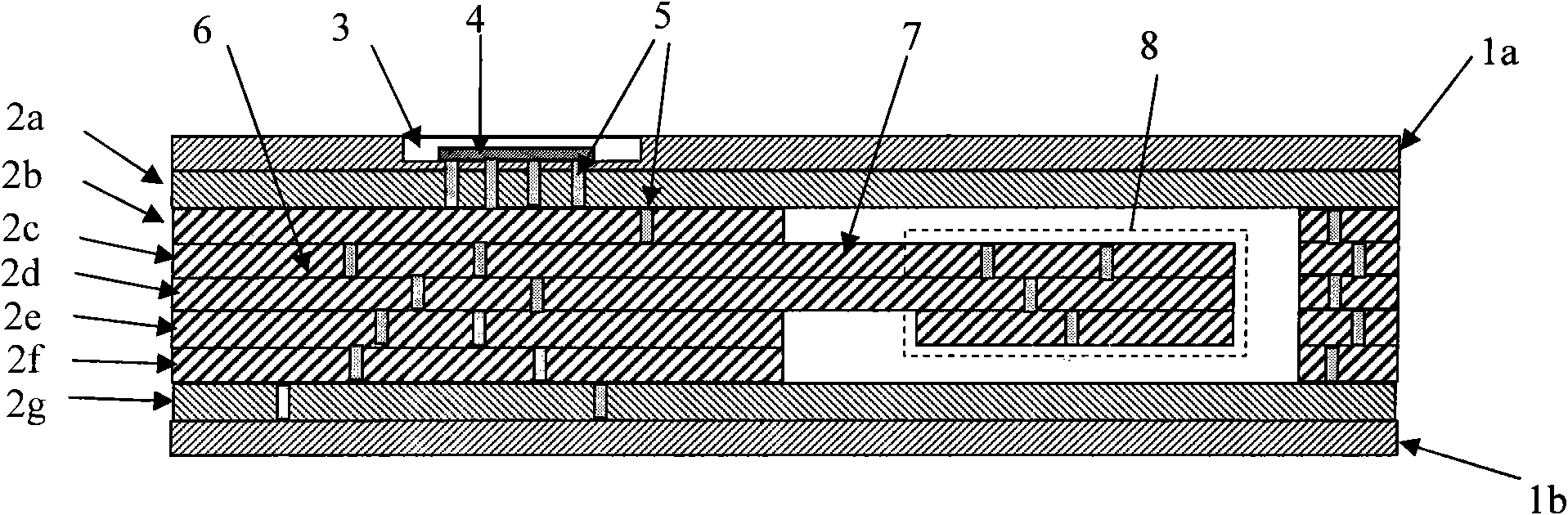
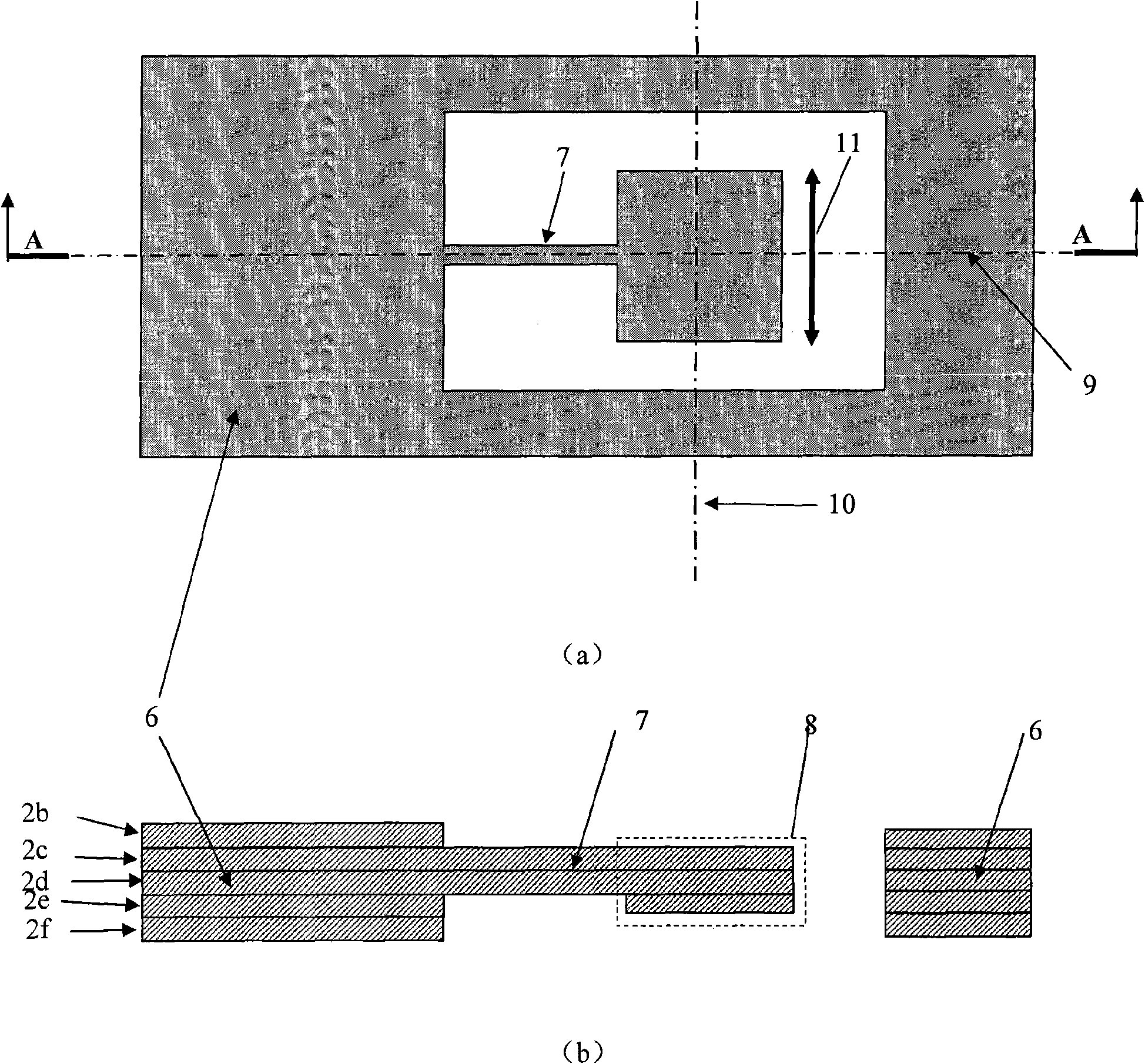
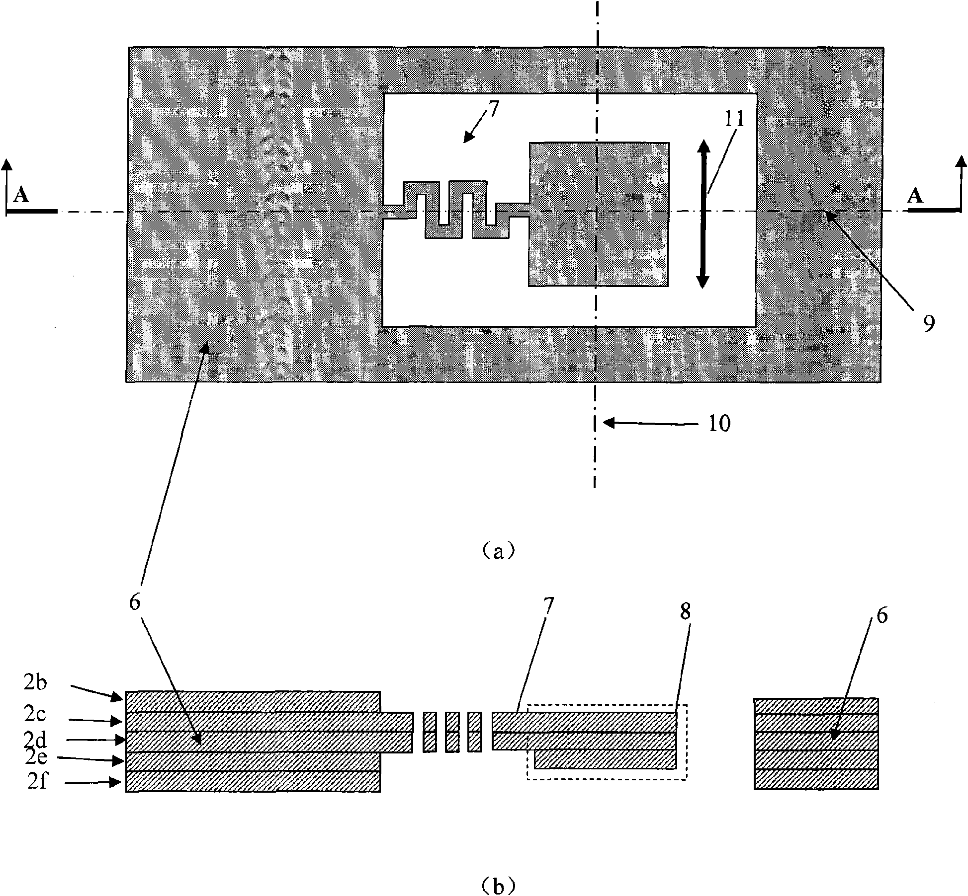
[0048] figure 1 A cross-sectional view of the basic structure of the sensitive element of the micro-accelerometer processed by the micro-inertial device manufacturing method of the present invention is shown. The multilayer packaging substrate in the figure is formed by stacking flat upper surface board 1a, lower surface board 1b and 2a~g and other intermediate substrates. The materials are all LTCC, and become an integrated multilayer packaging substrate after sintering process. The signal detection circuit 4 can adopt a commercialized, general-purpose accelerometer signal detection circuit chip, or a specially designed signal detection circuit chip, which can be attached to the metal surface at the bottom of the groove 3 on the upper surface plate 1a. On the pads, the chip is electrically interconnected with the sensitive element through thes...


PUM

PropertyMeasurementUnit
thicknessaaaaaaaaaa
thicknessaaaaaaaaaa

Abstract

The invention discloses a micro-accelerometer and a preparation method thereof, belonging to the technical field of processing micro inertia devices. The micro-accelerometer is arranged on a package substrate which is formed by stacking an upper surface plate, a lower surface plate and a plurality of middle substrates, wherein a signal detection circuit of the micro-accelerometer is attached on the upper surface plate; a sensitive element of the micro-accelerometer is embedded in the middle substrates, i.e. the middle substrates with cavities form a frame of the sensitive element; a flexible hanger and a sensitive mass block of the sensitive element are arranged in the cavities, and one end of the flexible hanger is connected with the sensitive element, while the other end is fixed on the frame; metal electrodes are respectively sputtered on the sensitive mass block and the surface of the frame corresponding to the sensitive mass block so as to form a flat plate sensitive capacitor, or a metal piezoresistive thick-film pattern is deposited at a connecting part of the flexible hanger and the inner side surface of the frame so as to form a metal piezoresistive strain gauge. The micro-accelerometer has high sensitivity and high-temperature resistance and can be fused into a whole with a system level package substrate, thus the micro-accelerometer has low processing difficulty and cost.

Description

technical field [0001] The invention relates to the processing technology of a micro-inertial device, in particular to a micro-accelerometer and a preparation method thereof. Background technique [0002] Micro-inertial devices mainly include micro-accelerometers and micro-gyroscopes. Due to their outstanding advantages such as small size, light weight, high measurement accuracy, low price per piece, and easy parallel manufacturing, they are favored by governments, military and military science and technology research institutions or companies. of great importance. Micro-inertial devices have been widely used in tactical missile / smart projectile mid-course guidance, smart bomb guidance and attitude control, UAV guidance and other occasions. In the civilian field, medium and low-precision micro-accelerometers have also been commercially applied in consumer electronics fields such as automobile attitude and driving control, industrial equipment motion monitoring, health monit...

Claims


Application Information

Patent Timeline
Patent Type & Authority Applications(China)
IPC IPC(8): G01P15/125G01P15/12B81B7/02B81C1/00B81C3/00B81C5/00
Inventor 缪旻张杨飞张静金玉丰
Owner PEKING UNIV
Why Eureka
Try Eureka