Nanometer electronic device based on semiconductor nano materials and preparation method thereof

A technology of nanoelectronic devices and nanomaterials, applied in the field of nanoelectronic devices, can solve problems such as difficult large-scale application, difficult carbon nanotubes, poor wettability of metals and carbon nanotubes, etc., and achieves a simple and easy preparation method Effect

Inactive Publication Date: 2010-04-07
PEKING UNIV
View PDF1 Cites 3 Cited by
  • Summary
  • Abstract
  • Description
  • Claims
  • Application Information

AI Technical Summary

Problems solved by technology

However, the performance of n-type devices reported by the first method is generally poor, and the on-off current ratio and on-state current value are relatively small, mainly because the metals with low work function used do not form well with carbon nanotubes. On the one hand, it may be that the wettability between the metal and the carbon nanotubes is not good, and the metal coating cannot form a good physical contact with the carbon nanotubes. On the other hand, most low work function metals have high chemical activity. It is easy to form an oxide layer on the surface (generally, the work function is higher), and these metal targets with oxides are easy to form compound-doped metal contacts in the coating process, or the vacuum degree is not high during the coating process. Oxidation of metal atoms also makes it difficult to form high-performance n-type contacts
Therefore, it is generally believed that it is difficult to use metals with low work function as contact electrodes to realize n-type devices with ohmic contacts of carbon nanotubes.
Although the second method can obtain n-type devices with better performance, because carbon tubes do not have dangling bonds, and doping with high chemical activity such as potassium is not stable, the device must be in a certain chemical environment. When the environment (such as When the temperature and atmosphere) change, the performance of the device changes accordingly, and the practicability is poor
However, due to the relatively low output of metal scandium, the cost is high, which is about 5 times the price of gold, and it is difficult to apply it on a large scale in the industry.

Method used


Image

  • Nanometer electronic device based on semiconductor nano materials and preparation method thereof
  • Nanometer electronic device based on semiconductor nano materials and preparation method thereof
  • Nanometer electronic device based on semiconductor nano materials and preparation method thereof

Examples


Embodiment 1

[0026] Embodiment 1: A single-walled carbon nanotube field-effect transistor with a bottom-gate structure using yttrium (Y) as the source-drain electrode and its preparation

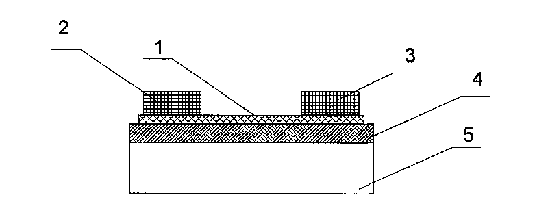
[0027] Such as figure 1 shown in SiO 2 It is a single-walled carbon nanotube field-effect transistor with a gate dielectric 4 and a back gate 5 structure using Si, and its source (S) 2 and drain (D) 3 electrode materials are yttrium (Y), which are located at the side of the single-walled carbon nanotube 1 ends. Concrete preparation steps are as follows:

[0028] 1) By positioning growth, or dropping the dispersed carbon tube solution onto the substrate, the Si / SiO 2 carbon nanotubes on a substrate;

[0029] 2) Observing with a scanning electron microscope or an atomic force microscope, and recording the specific position of the carbon nanotubes;

[0030] 3) Coating photoresist on the carbon nanotube and forming the shape of the electrode by optical exposure or electron beam lithography;

[0031] 4)...

Embodiment 2

[0036] Example 2: Carbon nanotube field effect transistor with Y as the top gate structure and its preparation

[0037] Such as Figure 4 In the carbon nanotube field effect transistor with Y as the top gate structure shown, the source (S) 8 and drain (D) 10 electrode materials are all yttrium (Y), and the electrode material of the gate (G) 6 is Ti. Walled carbon nanotubes 11 located in HfO 2 Under the gate dielectric layer 7, SiO 2 9 and Si12 on the substrate. Concrete preparation comprises the following steps:

[0038] 1) By positioning growth, or dropping the dispersed carbon tube solution onto the substrate to obtain the Si / SiO 2 carbon nanotubes on a substrate;

[0039] 2) Observing and recording the specific position of the carbon nanotubes through a scanning electron microscope or an atomic force microscope;

[0040] 3) Apply photoresist and form the shape of source and drain electrodes by optical exposure or electron beam lithography;

[0041] 4) Put the photoli...


PUM

PropertyMeasurementUnit
Saturation currentaaaaaaaaaa

Abstract

The invention discloses a nanometer electronic device based on semiconductor nano materials and a preparation method thereof; yttrium metal with low work function is adopted as a contact electrode material, the yttrium metal forms ohmic contact with a conduction band of one-dimensional semiconductor nanometer material directly, so as to obtain an electronic form field effect transistor with high performance and other nanometer electronic devices including a diode, biological and chemical sensors and the like, which take the semiconductor nanometer material as a base. The invention greatly reduces the processing cost of the nanometer type devices and circuits, improves the performance of the devices, and has very important significance for promoting the practical process of the nanometer electronic devices and has wide application prospect.

Description

technical field [0001] The invention relates to the field of nanoelectronic devices, in particular to a nanoelectronic device based on semiconductor nanomaterials, especially carbon nanotubes, and a method for realizing high-performance n-type contact between semiconductor nanomaterials and metal electrodes. Background technique [0002] The research of nanoelectronic devices is the most important field in today's nanotechnology. One-dimensional or quasi-one-dimensional semiconductor nanomaterials have unique electrical and optical properties, especially semiconductor nanomaterials represented by carbon nanotubes are considered to be one of the most promising building materials for nanoelectronic devices due to their unique electrical properties. one. So far, various nanoelectronic devices such as field-effect transistors (FETs), diodes, logic operation circuits, oscillators, decoders, infrared light-emitting devices, photodetectors, biological and chemical sensors, etc. ha...

Claims


Application Information

Patent Timeline
IPC IPC(8): H01L29/78H01L29/43H01L29/12H01L21/336H01L21/28H01L21/283H01L29/861H01L21/329C23C14/14
Inventor 王胜张志勇彭练矛丁力梁学磊陈清
Owner PEKING UNIV
Why Eureka
Try Eureka