Photoelectric conversion apparatus and method for manufacturing the same

A technology of photoelectric conversion device and manufacturing method, which is applied in the direction of cable/conductor manufacturing, photovoltaic power generation, circuits, etc., which can solve the problems of increased photoelectric conversion efficiency, reduced transmittance, difficulty in balancing resistivity and transmittance, etc., to achieve photoelectric conversion Increased efficiency, improved interface properties, and stable photoelectric conversion efficiency

Inactive Publication Date: 2010-08-04
MITSUBISHI HEAVY IND LTD
View PDF1 Cites 0 Cited by
  • Summary
  • Abstract
  • Description
  • Claims
  • Application Information

AI Technical Summary

Problems solved by technology

[0006] However, although gallium oxide or aluminum oxide is added to achieve low resistance of the transparent electrode, there is a problem that the transmittance decreases.
In this way, even if Ga or Al is added to the oxide-based transparent conductive film, the resistivity and transmittance show opposite characteristics, and it is difficult to achieve both resistivity and transmittance.
[0007] In addition, in the above-mentioned Patent Document 1, in a solar cell in which the photoelectric conversion layer is made of amorphous silicon, when 0.5 atomic % of Ga is added to Zn in a transparent conductive film mainly composed of ZnO, there is no difference between Compared with the case where Ga is added, the data show that the photoelectric conversion efficiency is increased (Example 4 to Example 6 in Table 2), but this technology is only for the purpose of lowering the temperature when forming a transparent conductive film. Research
That is to say, the above technology does not pay attention to the effect of Ga addition on the interface characteristics between the photoelectric conversion layer and the transparent electrode composed of Ga-added ZnO, and the effect on the resistivity and transmittance of Ga-added ZnO. , not to study the amount of Ga added with the aim of increasing the photoelectric conversion efficiency

Method used


Image

  • Photoelectric conversion apparatus and method for manufacturing the same
  • Photoelectric conversion apparatus and method for manufacturing the same
  • Photoelectric conversion apparatus and method for manufacturing the same

Examples


no. 1 approach

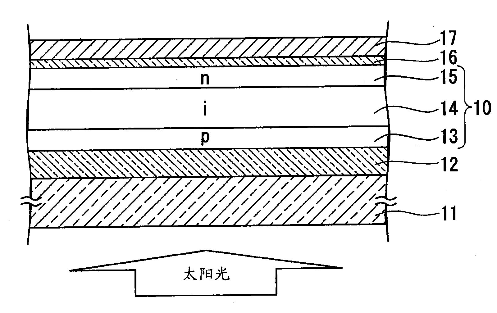
[0042] Below, use figure 1 A photoelectric conversion device according to a first embodiment of the present invention will be described.

[0043] The photoelectric conversion device of the present embodiment is a photoelectric conversion device of a type (also referred to as a "overhead type") in which the photoelectric conversion layer 10 is made of amorphous silicon and light enters from a transparent insulating substrate.

[0044] (first process)

[0045] The first transparent electrode 12 is formed on the transparent insulating substrate 11 . For the transparent insulating substrate 11 , for example, white glass showing light transmission is used.

[0046] As the first transparent electrode 12, SnO 2 (tin oxide).

[0047] Set the transparent insulating substrate 11 in the atmospheric pressure thermal CVD device, with SnCl 4 , water vapor (H 2 O), anhydrous hydrogen fluoride (HF) as raw material gas, make SnO 2 A film is formed on the transparent insulating substrate...

no. 2 approach

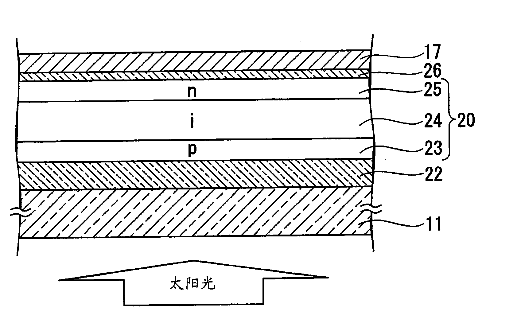
[0076] Use the following figure 2 A photoelectric conversion device according to a second embodiment of the present invention will be described.

[0077] The photoelectric conversion device of the present embodiment is a photoelectric conversion device of the type in which the photoelectric conversion layer 20 is made of microcrystalline silicon and light enters from a transparent insulating substrate. The photoelectric conversion device of this embodiment is a photoelectric conversion device of the type (overhead type) in which the power generation layer is made of microcrystalline silicon, but light enters from a transparent insulating substrate as in the first embodiment.

[0078] (first process)

[0079] The first transparent electrode 22 is formed on the transparent insulating substrate 11 . For the transparent insulating substrate 11 , for example, white glass showing light transmission is used.

[0080] As the first transparent electrode 22, SnO 2 (tin oxide).

[...

no. 3 approach

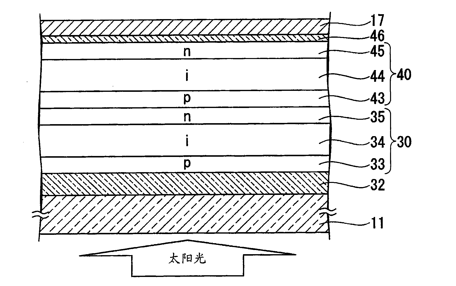
[0107] Use the following image 3 A photoelectric conversion device according to a third embodiment of the present invention will be described.

[0108] The photoelectric conversion device of this embodiment differs from the above-mentioned embodiments in that the photoelectric conversion layer is a layer in which a photoelectric conversion layer 30 (second photoelectric conversion layer) made of amorphous silicon and a photoelectric conversion layer 30 made of microcrystalline silicon are laminated. Layer 40 (first photoelectric conversion layer) is a tandem photoelectric conversion device. The photoelectric conversion device of this embodiment is the same as the first and second embodiments in that it is a photoelectric conversion device of a type (overhead type) in which light enters from a transparent insulating substrate.

[0109] (first process)

[0110] The first transparent electrode 32 is formed on the transparent insulating substrate 11 . For the transparent insul...


PUM

PropertyMeasurementUnit
electrical resistivityaaaaaaaaaa
transmittivityaaaaaaaaaa

Abstract

This invention provides a photoelectric conversion apparatus, which can realize a stably high photoelectric conversion efficiency using a transparent electrode having an optimized relationship between electrical resistivity and transmittance, and a method for manufacturing the same. At least one of transparent electrodes (12, 16) is formed of a Ga-free ZnO layer or a Ga-added ZnO layer. The content of Ga in the ZnO layer is not more than 5 atomic% based on Zn in the ZnO layer. The ZnO layer is formed by a sputtering method using an oxygen-containing rare gas as a sputtering gas. The content of oxygen in the sputtering gas is not less than 0.1% by volume and not more than 5% by volume based on the total volume of the oxygen and rare gas.

Description

technical field [0001] The present invention relates to a photoelectric conversion device including a transparent electrode mainly containing ZnO (zinc oxide) and a method for manufacturing the same. Background technique [0002] Conventionally, silicon-based thin-film photoelectric conversion devices are known as photoelectric conversion devices such as solar cells. In this photoelectric conversion device, generally, a first transparent electrode, a silicon-based semiconductor layer (photoelectric conversion layer), a second transparent electrode, and a metal electrode film are sequentially stacked on a substrate. [0003] As a transparent electrode, it is required to use materials with low resistance and high transmittance, usually ZnO (zinc oxide), SnO 2 (tin oxide), ITO (indium oxide tin oxide composite oxide) and other oxide-based transparent conductive films. In order to realize such a low resistance of the transparent electrode, gallium oxide, aluminum oxide, fluori...

Claims


Application Information

Patent Timeline
Patent Type & Authority Applications(China)
IPC IPC(8): H01L31/042C23C14/08H01B5/14H01B13/00
CPCH01L31/0527H01L31/022466C23C14/086Y02E10/52H01L31/076C23C14/0036H01L31/075Y02E10/548Y02E10/50H01L31/1884H01L31/022483H01L31/056
Inventor 山下信树渡边俊哉坂井智嗣中野要治
Owner MITSUBISHI HEAVY IND LTD
Why Eureka
Try Eureka