Method for preparing GaN-based pattern substrate template based on anodized aluminum

A technology of anodized aluminum and graphic substrates, which is applied in semiconductor/solid-state device manufacturing, electrical components, circuits, etc., can solve the problems of complex process, expensive equipment, and high cost, and achieve simple process, easy production and mass production, and low cost. low effect

Inactive Publication Date: 2010-08-18
SUN YAT SEN UNIV
View PDF2 Cites 12 Cited by
  • Summary
  • Abstract
  • Description
  • Claims
  • Application Information

AI Technical Summary

Problems solved by technology

Substrates with smaller pattern sizes are usually prepared by electron beam lithography or X-ray lithography, but these a...

Method used


Image

  • Method for preparing GaN-based pattern substrate template based on anodized aluminum
  • Method for preparing GaN-based pattern substrate template based on anodized aluminum
  • Method for preparing GaN-based pattern substrate template based on anodized aluminum

Examples


Embodiment Construction

[0038] The present invention will be further described below in conjunction with the accompanying drawings.

[0039] The preparation method of the GaN-based pattern substrate template based on anodized aluminum of the present invention comprises the following steps:

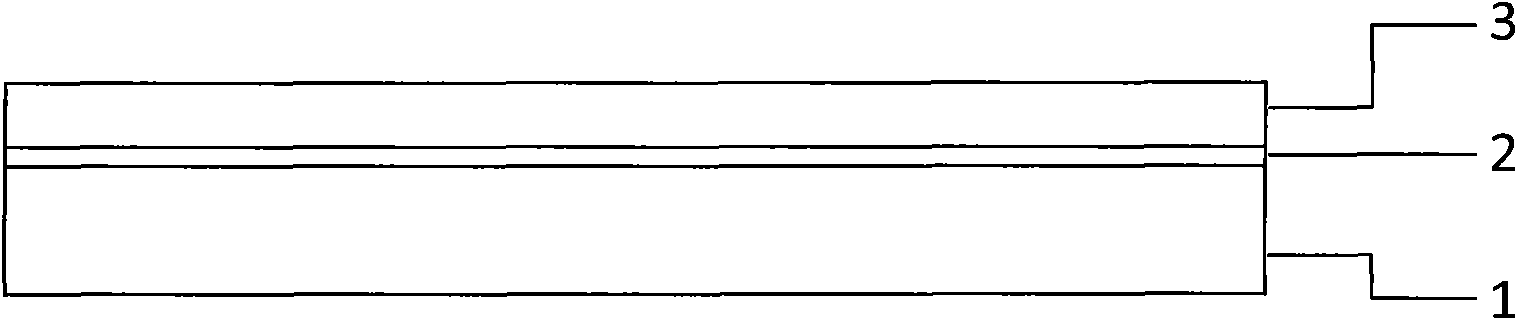
[0040] Step (1): A GaN film with a thickness of 2 micrometers is grown on the sapphire substrate 1 by MOCVD as a GaN template 2 for nitride growth. Then deposit a thin layer of aluminum 3 with a thickness of 4 microns on the surface of the GaN template 2, such as figure 1 .

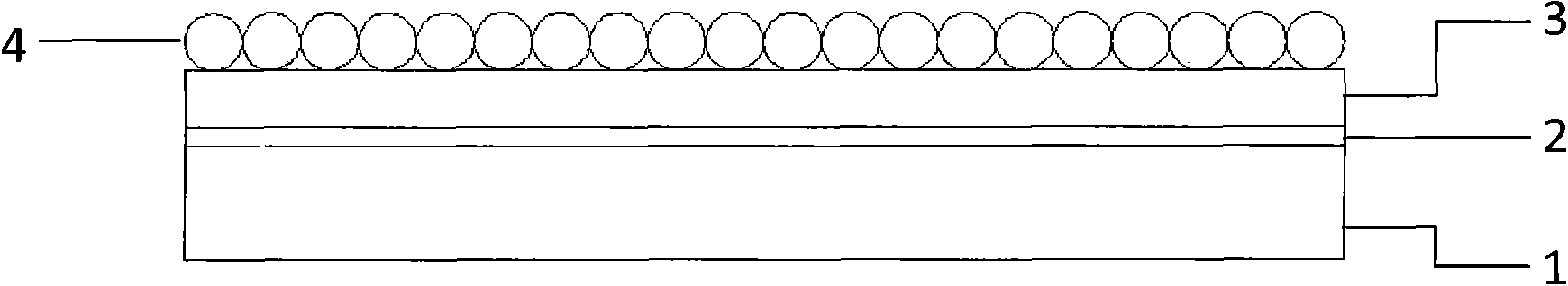
[0041] Step (2): Mix polystyrene microspheres and ethanol to prepare a mixed solution, and spin-coat the mixed solution on the surface of the thin aluminum layer 3 to form the microsphere layer 4 . Polystyrene spheres aggregate into a monolayer structure, such as figure 2 .

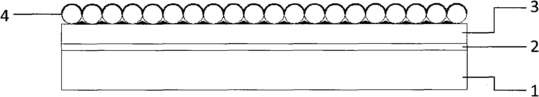
[0042] Step (3): 10nm nickel is deposited on the polystyrene microsphere layer 4, and the nickel passes through the gap between the microspheres to deposit on the ...


PUM


Abstract

The invention relates to a method for preparing a GaN-based pattern substrate template based on anodized aluminum. The method comprises the following steps: growing a GaN-based template on a substrate; depositing an aluminium layer on the GaN-based template; laying a microsphere layer on the surface of the aluminum layer; performing metal evaporation on the substrate; removing the microsphere layer in a monolayer structure through ultrasonic vibration to obtain a patterned metal layer; etching pits on the surface of the aluminium layer by utilizing the metal layer as a mask; removing the metal layer and forming a porous aluminium oxide layer; transferring the pattern on the aluminium oxide layer to the GaN-based template by taking the porous aluminium oxide layer as the mask; and removing the porous aluminium oxide layer to obtain the GaN-based material pattern substrate template. The method for preparing a micron GaN-based pattern substrate has the characteristics of simple process, low cost and controllable size and distance of the pattern pits.

Description

technical field [0001] The invention relates to the field of semiconductor material growth, in particular to a method for preparing a GaN-based graphic substrate template based on anodized aluminum. Background technique [0002] Nitride compound semiconductor materials represented by III-V gallium nitride (GaN) materials are widely used in violet light-emitting diodes, violet lasers, ultraviolet light detectors, and high-power high-frequency electronic devices. Due to the lack of suitable substrate materials, the current epitaxy of high-quality GaN-based materials is grown on heterogeneous substrates such as sapphire, SiC, and Si. However, there is a large lattice mismatch and thermal expansion coefficient mismatch between the heterogeneous substrate and GaN-based materials. This will result in a large stress and crystal defect density in GaN-based material epitaxial layers grown by epitaxial techniques such as metal organic chemical vapor deposition (MOCVD), hydride vapor ...

Claims


Application Information

Patent Timeline
IPC IPC(8): H01L21/02
Inventor 张佰君卫静婷饶文涛
Owner SUN YAT SEN UNIV
Why Eureka
Try Eureka