Multichannel carbon nanotube sensor and preparation method thereof

A carbon nanotube and carbon nanotube composite technology, which is applied in the field of microelectronics, can solve the problems of poor IC integrated circuit compatibility, poor reliability, weak current, etc., and achieve improved reliability and stability, stable and reliable combination, and high detection sensitivity Effect

Inactive Publication Date: 2010-10-27
SHANGHAI JIAO TONG UNIV
View PDF4 Cites 8 Cited by
  • Summary
  • Abstract
  • Description
  • Claims
  • Application Information

AI Technical Summary

Problems solved by technology

Such sensors use a single carbon nanotube to conduct electricity, have poor reliability and weak current, and cannot be extended to large-scale integrated manufacturing and use.
The Chinese patent application No. 200680048146.7 proposes a carbon nanotube interdigital sensor, which realizes the connection between the two ends of multiple horizontal carbon nanotubes and the metal interdigital electrode, and in situ on the basis of the connection between the metal catalyst itself and the carbon nanotube To make electrodes, but this method utilizes the unreliable contact between the grown carbon nanotubes and the electrodes, poor compatibility with IC integrated circuits, and the horizontal arrangement of carbon tubes is not conducive to the improvement of devices and large-scale integration

Method used


Image

  • Multichannel carbon nanotube sensor and preparation method thereof
  • Multichannel carbon nanotube sensor and preparation method thereof
  • Multichannel carbon nanotube sensor and preparation method thereof

Examples


preparation example Construction

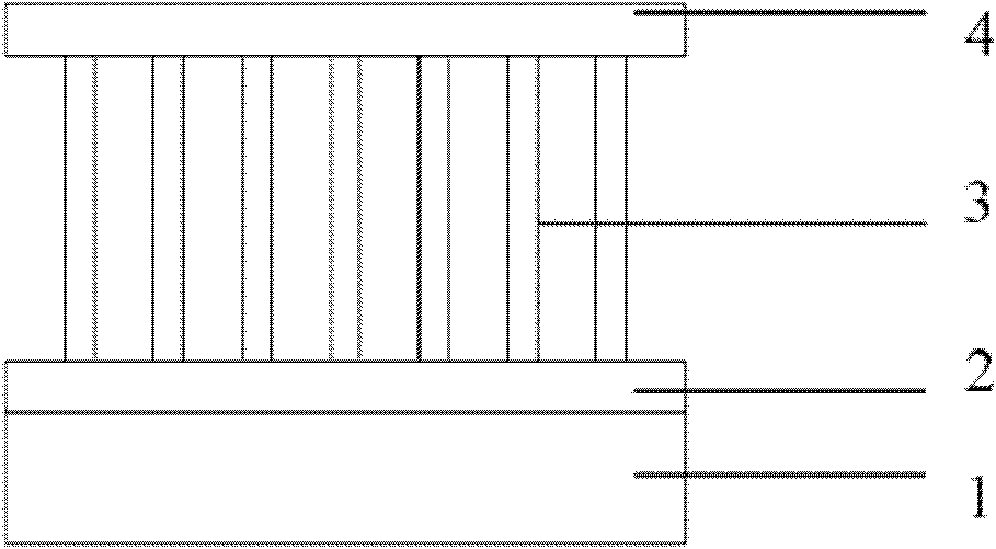
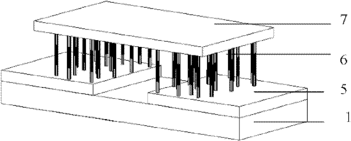
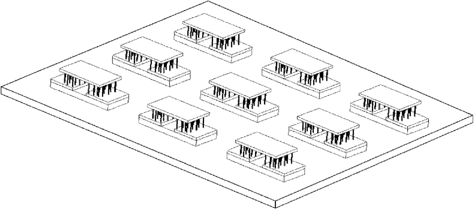
[0045] 1. Utilize the common PECVD method (plasma-enhanced chemical vapor deposition method) for preparing carbon nanotube field emission cathode arrays to obtain uniformly oriented multi-walled carbon nanotube arrays on silicon wafers deposited with nickel metal catalysts, using conventional photolithography The patterning process enables the nickel catalyst to be patterned on the silicon wafer, thereby realizing the patterning treatment of the conductive channel of the carbon nanotube, and the length of the carbon nanotube is 10 μm;

[0046] 2. Spin-coat the photoresist on the substrate to cover the carbon nanotube array. The thickness of the photoresist is 15 μm, bake the glue, and grind the photoresist with sandpaper so that the thickness of the photoresist is about 8 μm

[0047] 3. Use a sodium hydroxide solution with a concentration of 0.5% to control the etching of the photoresist for 30 seconds; 4. Deposit a Cr / Cu seed layer on the surface of the above structure, wherei...

Embodiment 2

[0056] 1. Utilize the common PECVD method (plasma-enhanced chemical vapor deposition method) for preparing carbon nanotube field emission cathode arrays to obtain uniformly oriented multi-walled carbon nanotube arrays on silicon wafers deposited with iron metal catalysts. The length is 10 μm;

[0057] 2. Spin-coat the photoresist on the substrate to cover the carbon nanotube array. The thickness of the photoresist is 15 μm, bake the glue, and grind the photoresist with sandpaper so that the thickness of the photoresist is about 8 μm

[0058] 3. Conduct photolithographic patterning on the conductive channel of carbon nanotubes. After removing the glue, perform RIE etching to remove the exposed carbon nanotubes, and fill them with spin-coated photoresist;

[0059] 4. Use a sodium hydroxide solution with a concentration of 0.6% to perform controlled etching on the photoresist for 25 seconds;

[0060] 5. Deposit a Cr / Cu seed layer on the surface of the above structure, wherein th...

Embodiment 3

[0069] The carbon nanotube sensor preparation process based on the carbon nanotube finished product is as follows:

[0070] 1. Purify the multi-walled carbon nanotubes with a length of 10 μm obtained by the usual preparation method, mix them with photoresist in proportion, the mass ratio of carbon nanotubes and photoresist is 1:8, and mix them with a ball mill for 5 Hour;

[0071] 2. Spin-coat 8 μm photoresist on the silicon wafer and pattern it, then spin-coat the mixture of photoresist and carbon nanotubes, fill and cover the patterned photoresist pattern, dry it, and grind it with sandpaper until Expose the first layer of photoresist;

[0072] 3. Use a sodium hydroxide solution with a concentration of 0.4% to perform controlled etching on the photoresist for 40 seconds;

[0073] 4. Deposit a Cr / Cu seed layer on the surface of the above structure, wherein the thickness of Cr Cu thickness is

[0074] 5. Spin-coat photoresist on the above-mentioned Cr / Cu seed layer and ...


PUM

PropertyMeasurementUnit
thicknessaaaaaaaaaa
depthaaaaaaaaaa
depthaaaaaaaaaa

Abstract

The invention relates to a multichannel carbon nanotube sensor, which belongs to the technical field of micro-electronics, and a preparation method thereof. The multichannel carbon nanotube sensor comprises a substrate, a lower metal electrode, carbon nanotubes and an upper metal electrode, wherein the substrate is arranged on the bottommost end of the integral structure, the lower metal electrode is arranged on the substrate, a plurality of carbon nanotubes are vertically distributed to form an array, and the two ends of each carbon nanotube are respectively connected with the lower metal electrode and the upper metal electrode to form carbon nanotube conducting channels. The lower metal electrode, the carbon nanotube conducting channels and the upper metal electrode form a plurality of series unit structures. The sensor prepared in the invention can realize up-and-down integration, is compatible with the IC integrated circuit, can be used to manufacture array sensors and realize diversified and integrated manufacture of the devices.

Description

technical field [0001] The invention relates to a device and a preparation method in the technical field of microelectronics, in particular to a multi-channel carbon nanotube sensor and a preparation method thereof. Background technique [0002] As the primary link to realize automatic detection and automatic control systems, sensors have widely penetrated into fields such as industrial production, environmental protection, medical diagnosis, and bioengineering. The development of modern sensors depends on the development of new materials and sensitive components for sensor technology, and the application of semiconductors and dielectric materials is the main trend of development. Since the discovery of carbon nanotubes (CNTs) by Iijima in 1991, their unique physical and chemical properties such as unique metallic semiconductor conductivity mechanism and semiconductor properties, good adsorption capacity, more catalytic active sites, larger Specific surface area, extremely ...

Claims


Application Information

Patent Timeline
Patent Type & Authority Applications(China)
IPC IPC(8): B81B7/02B81C1/00
Inventor 丁桂甫陆闻静王艳邓敏周镇威
Owner SHANGHAI JIAO TONG UNIV
Why Eureka
Try Eureka