Manufacture method of semiconductor device

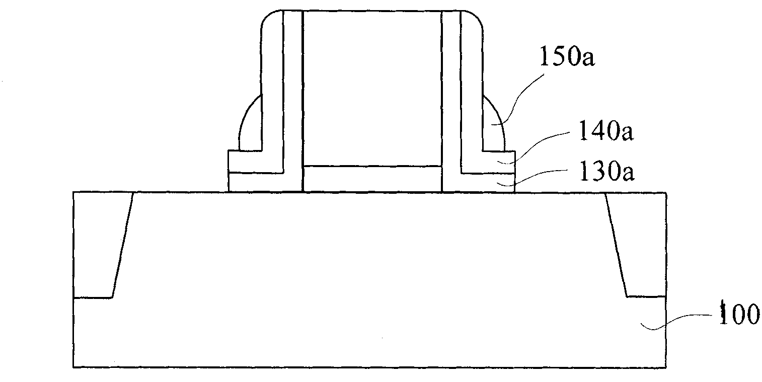
A manufacturing method and semiconductor technology, applied in semiconductor/solid-state device manufacturing, semiconductor devices, electrical components, etc., can solve problems such as lowering product yield, semiconductor device failure, and corrosion of the first oxide layer 130a, so as to ensure quality and speed up Etching rate, the effect of improving electrical properties

Active Publication Date: 2010-10-27
SHANGHAI HUAHONG GRACE SEMICON MFG CORP
View PDF4 Cites 4 Cited by
  • Summary
  • Abstract
  • Description
  • Claims
  • Application Information

AI Technical Summary

Problems solved by technology

[0012] However, since the remaining second oxide layer 150a remains at the corner of the sidewall layer, and after the wet etching process, the remaining second oxide layer 150a cannot be completely removed.
Therefore, during the argon ion sputtering step, these residual second oxide layers may be deposited on the silicon surface again, hindering the formation of salicides, thereby affecting the quality of salicides, resulting in Semiconductor devices fail, reducing product yield
The industry has tried various methods to solve the above problems, for example, prolonging the time of the wet etching step, but this will cause the patterned first oxide layer 130a to be corroded as well.
In addition, the industry has tried to reduce the thickness of the second oxide layer, but this will affect the critical dimension (CD) of the formed sidewall layer, which in turn will affect the electrical performance of the semiconductor device

Method used


Image

  • Manufacture method of semiconductor device
  • Manufacture method of semiconductor device
  • Manufacture method of semiconductor device

Examples


Embodiment Construction

[0027] The core idea of ​​the present invention is to provide a manufacturing method of a semiconductor device. In the method, after forming the sidewall layer and before performing the wet etching process, the process step of argon ion implantation is added. The argon ion implantation process will make the sidewall layer The remaining second oxide layer at the corner of the wall layer is amorphized, thereby accelerating the etching rate of the second oxide layer in the wet etching process, ensuring that the remaining second oxide layer at the corner of the side wall layer is completely removed, and ensuring the final formation The quality of self-aligned metal silicide, thereby improving the electrical performance of semiconductor devices.

[0028] Please refer to figure 2 , which is a flow chart of a method for manufacturing a semiconductor device provided by an embodiment of the present invention. In combination with this figure, the method includes the following steps:

...


PUM


Abstract

The invention discloses a manufacture method of a semiconductor device, comprising the following steps of: providing a semiconductor substrate on which a grid electrode is formed; forming a first oxidation layer, a silicon nitride layer and a second oxidation layer on the semiconductor substrate and the grid electrode in sequence; etching the second oxidation layer, the silicon nitride layer and the first oxidation layer until the top of the grid electrode is exposed to form a side wall layer; executing an argon ion implantation process; executing a wet etching process; forming a source electrode and a drain electrode in the semiconductor substrate at both sides of the side wall layer; forming self-aligned blocking layers on the surfaces of the semiconductor substrate, the side wall layer and the grid electrode, wherein the self-aligned blocking layers are provided with openings for exposing the grid electrode, the source electrode and the drain electrode; executing an argon ion sputtering process; and forming self-aligned metal silicides on the surfaces of the grid electrode, the source electrode and the drain electrode. According to the invention, the second oxidation layer remaining at the corners of the side wall layer can be removed effectively to ensure the quality of the self-aligned metal silicides and improve the electrical behavior of the semiconductor device.

Description

technical field [0001] The invention relates to the field of integrated circuit manufacturing, in particular to a manufacturing method of a semiconductor device. Background technique [0002] Self-aligned metal silicide (Salicide) has low resistivity and has good adhesion properties with silicon, and is widely used in source, drain contact layer and gate contact layer to reduce contact resistance. Metal suicides can be formed by the reaction of refractory metals and silicon. With the decreasing size of semiconductor devices, the requirements for the performance of semiconductor devices are getting higher and higher, especially for technology nodes of 90nm and below. In order to obtain lower contact resistance, the industry uses metals such as cobalt, nickel or titanium as the form Low resistivity salicide metal material. [0003] For details, please refer to Figure 1A to Figure 1H , which is a schematic cross-sectional view of structures corresponding to each step of a co...

Claims


Application Information

Patent Timeline
IPC IPC(8): H01L21/336H01L21/28H01L21/768
Inventor 肖海波
Owner SHANGHAI HUAHONG GRACE SEMICON MFG CORP
Why Eureka
Try Eureka