Organic photoelectric device and preparation method thereof

An optoelectronic device and organic technology, applied in the field of organic optoelectronic devices and their preparation, can solve problems such as low conductivity, lower device energy conversion efficiency, and difficulty in effective charge transmission, so as to increase light absorption, increase visible light transmittance, The effect of increasing the external quantum efficiency

Inactive Publication Date: 2010-11-10
UNIV OF ELECTRONICS SCI & TECH OF CHINA
View PDF4 Cites 40 Cited by
  • Summary
  • Abstract
  • Description
  • Claims
  • Application Information

AI Technical Summary

Problems solved by technology

However, due to the low conductivity of organic materials, it is difficult for the charges generated at the D-A int...

Method used


Image

  • Organic photoelectric device and preparation method thereof
  • Organic photoelectric device and preparation method thereof
  • Organic photoelectric device and preparation method thereof

Examples


Embodiment 1

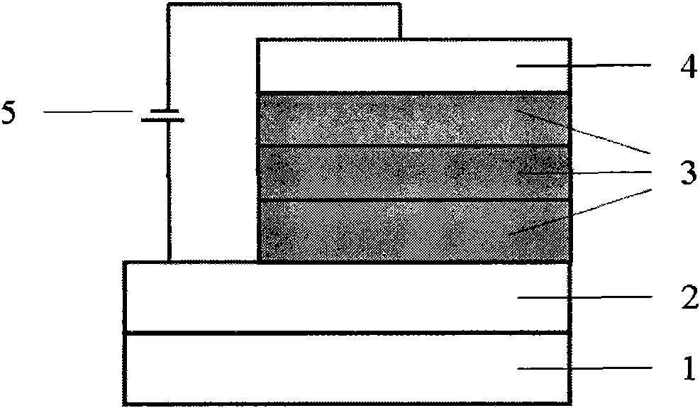
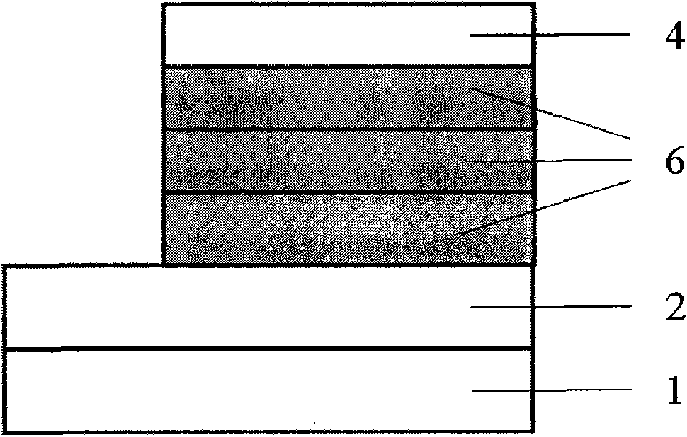
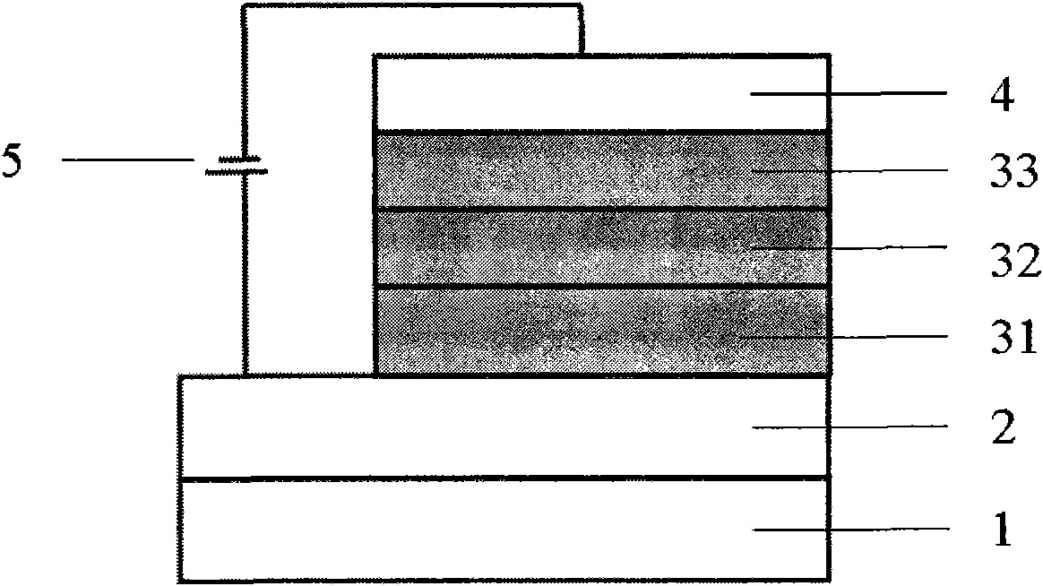
[0077] Such as image 3 As shown, the substrate 1 of the device is transparent glass, the anode layer 2 is ITO, and the material of the hole transport layer 31 is Fe doped with a uniform surface distribution diameter of 10 nm. 3 o 4 The NPB of multi-walled carbon nanotubes of particles, the material of light-emitting layer 32 is Alq 3 , The electron transport layer 33 is made of BCP, and the cathode layer 4 is made of Mg:Ag alloy. The entire device structure is described as:

[0078] Glass substrate / ITO / NPB: magnetic multi-walled carbon nanotubes (15%, 50nm) / Alq 3 (20nm) / BCP(40nm) / Mg:Ag(100nm)

[0079] The preparation method is as follows:

[0080] ①Use acetone, ethanol solution and deionized water to ultrasonically clean the transparent conductive substrate ITO glass, and dry it with dry nitrogen after cleaning. The ITO film on the glass substrate is used as the anode layer of the device, the square resistance of the ITO film is 15Ω / □, and the film thickness is 180nm; ...

Embodiment 2

[0089] Such as image 3 As shown, the substrate 1 of the device is transparent glass, the anode layer 2 is ITO, the material of the hole transport layer 31 is NPB, and the material of the light emitting layer 32 is Alq 3 , the material of the electron transport layer 33 is γ-Fe doped with a uniform surface distribution diameter of 15nm 2 o 3 Particles of single-walled carbon nanotubes of BPhen, cathode layer 4 made of Mg:Ag alloy. The entire device structure is described as:

[0090] Glass substrate / ITO / NPB(50nm) / Alq 3 (20nm) / BPhen: magnetic single-walled carbon nanotubes (10%, 50nm) / Mg:Ag(100nm)

[0091] The preparation method is as follows:

[0092] ①Use acetone, ethanol solution and deionized water to ultrasonically clean the transparent conductive substrate ITO glass, and dry it with dry nitrogen after cleaning. The ITO film on the glass substrate is used as the anode layer of the device, the square resistance of the ITO film is 15Ω / □, and the film thickness is 180nm...

Embodiment 3

[0098] Such as image 3 As shown, the substrate 1 of the device is polyethylene terephthalate (PET), the anode layer 2 is ITO, the material of the hole transport layer 31 is PVK, the material of the light emitting layer 32 is PPV, and the material of the electron transport layer 33 is For BPhen doped with single-walled carbon nanotubes with cobalt particles uniformly distributed on the surface and with a diameter of 15 nm, the cathode layer 4 is made of Mg:Ag alloy. The entire device structure is described as:

[0099] PET / ITO / PVK(50nm) / PPV(20nm) / BPhen: magnetic single-walled carbon nanotubes (15%, 50nm) / Mg:Ag(100nm)

[0100] The preparation method is as follows:

[0101] ①Use acetone, ethanol solution and deionized water to ultrasonically clean the ITO-coated PET substrate, and dry it with dry nitrogen after cleaning. Among them, the ITO film on the PET substrate is used as the anode layer of the device, the square resistance of the ITO film is 15Ω / □, and the film thicknes...


PUM

PropertyMeasurementUnit
Lengthaaaaaaaaaa
Diameteraaaaaaaaaa
Diameteraaaaaaaaaa

Abstract

The invention discloses an organic photoelectric device, which comprises a substrate, an anode layer, a cathode layer, and an organic functional layer arranged between the anode layer and the cathode layer. The organic functional layer comprises one or more of a hole injection layer, a hole transmission layer, a luminous layer, an electron transmission layer, an electron injection layer, an anode buffer layer, an electron donor layer, an interface layer, an electron acceptor layer and an cathode buffer layer; the hole transmission layer and the electron donor layer are doped with magnetic multi-wall carbon nanotubes, or the electron transmission layer and the electro acceptor layer are doped with magnetic single-wall carbon nanotubes, or the hole transmission layer and the electron donor layer are doped with magnetic multi-wall carbon nanotubes and the electron transmission layer and the electron acceptor layer are doped with the magnetic single-wall carbon nanotubes simultaneously; and the length direction of the magnetic multi-wall carbon nanotubes and the magnetic single-wall carbon nanotubes is vertical to the surface of the anode layer. The device reduces the resistance of a carrier transmission layer, improves the carrier transmission capacity and the visible light transmissivity of the carrier transmission layer, and improves the photoelectric performance of the device.

Description

technical field [0001] The invention relates to the field of organic photoelectric technology in electronic components, in particular to an organic photoelectric device and a preparation method thereof. Background technique [0002] The organic photoelectric device in the present invention refers to a device that needs to use holes and / or electrons to perform energy exchange between electrodes and organic materials. The organic optoelectronic device can be roughly divided into the following two types according to its working principle: one type has excitons that flow into the device from an external light source to form excitons in the organic layer and the excitons are separated into electrons and holes, and the formed electrons and holes An optoelectronic device configured to be delivered to different electrodes and used as a power source. The other type is a photoelectric device with a configuration in which holes and / or electrons are injected into an organic semiconduct...

Claims


Application Information

Patent Timeline
IPC IPC(8): H01L51/42H01L51/46H01L51/50H01L51/54H01L51/48H01L51/56
CPCY02E10/549
Inventor 于军胜陈苏杰于欣格蒋亚东
Owner UNIV OF ELECTRONICS SCI & TECH OF CHINA
Why Eureka
Try Eureka