Plane-configured organic infrared or ultraviolet photovoltaic semiconductor detector

An organic ultraviolet light, planar configuration technology, applied in the field of optoelectronics, can solve the problems of not meeting the requirements of practical infrared detectors, limiting the application of infrared detectors, and the response band is not ideal, achieving low power consumption, reducing device costs, Easy to form array effects

Active Publication Date: 2011-02-16
KUNMING INST OF PHYSICS
View PDF5 Cites 12 Cited by
  • Summary
  • Abstract
  • Description
  • Claims
  • Application Information

AI Technical Summary

Problems solved by technology

[0006] At present, the practical quantum infrared detectors are mainly inorganic materials based on mercury cadmium telluride. The problems of these materials are: high preparation cost, complicated process, and cannot be prepared on cheap substrates, especially silicon substrates and metal electrodes. , thus limiting the application of infrared detectors with important military applications
[0009] The main problem of organic infrared semiconductor materials at present is that the response band is not ideal (up to 1.60um), and the infrared response band is still lower than the first infrared window, which does not meet the requirements of practical infrared detector materials.

Method used


Image

  • Plane-configured organic infrared or ultraviolet photovoltaic semiconductor detector
  • Plane-configured organic infrared or ultraviolet photovoltaic semiconductor detector
  • Plane-configured organic infrared or ultraviolet photovoltaic semiconductor detector

Examples


Embodiment 1

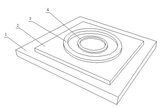
[0044] as attached image 3 As shown, a quartz plate is used as the substrate 1, and a 1 μm thick organic ultraviolet semiconductor anthracene 2 is deposited on the quartz substrate by thermal evaporation, and a high work function Au outer ring is deposited on the anthracene film by thermal evaporation with the help of a mask. Electrode 4, in which the width of the ring is 500 nm, and the thickness of the Au film is 300 nm. Similarly, a low work function yttrium inner ring electrode 3 is deposited on the anthracene film by thermal evaporation using a mask plate and precise alignment technology, wherein the width of the ring is 500 nm, and the thickness of the yttrium film is 300 nm.

[0045]

Embodiment 2

[0047] as attached Figure 4 As shown, a quartz plate is used as the substrate 1, and a 500nm high work function metal Au film is deposited on the quartz substrate by magnetron sputtering, and then the Au film is subjected to glue rejection, pre-baking, exposure, development, and film hardening. , etching, and glue removal to form the gold interdigitated right electrode 4, and then use a lift-off photolithography process to prepare a low work function metal yttrium interdigitated left electrode 3 with a thickness of 500 nm, dissolve the phenanthrene with cyclohexane, and absorb the phenanthrene with a dropper Cyclohexane solution, drop it on the interdigital electrode, and make the film thickness of phenanthrene reach 500nm after the solvent evaporates.

[0048]

Embodiment 3

[0050] as attached Figure 5 As shown, a glass sheet is used as a substrate 1, and a 1 μm-thick organic infrared semiconductor iodine-doped phthalocyanine erbium 2 is deposited on the glass substrate by thermal evaporation. Deposit high work function Au right strip electrode 4 on the erbium film, wherein the width of the Au strip is 500nm, the length of the Au strip is 2.5μm, and the thickness of the Au film is 300nm; Methods A low work function yttrium left strip electrode 3 was deposited on the iodine-doped erbium phthalocyanine film. The width of the yttrium strip was 500 nm, the length of the yttrium strip was 2.5 μm, and the thickness of the yttrium film was 300 nm.

[0051]


PUM


Abstract

The invention relates to the technical field of photoelectron, in particular to a plane-configured organic infrared or ultraviolet photovoltaic semiconductor detector which comprises a substrate, an organic infrared or ultraviolet photovoltaic semiconductor, a low work function electrode and a high work function electrode. The detector is characterized in that the low work function electrode and the high work function plane are in the same plane. The plane-configured organic infrared or ultraviolet photovoltaic semiconductor detector technology of the invention can be applied to manufacture a plane-configured organic infrared photovoltaic semiconductor detector and a plane-configured organic ultraviolet photovoltaic semiconductor detector. Compared with the optical waveguide detector, the detector of the invention has the advantages of fast response speed, low power dissipation, easy formation of array, no need of offsetting and the like. In addition, the detector of the invention has the characteristics of low cost, easy realization of controllable electrical resistivity of large area photosensing materials, no need of refrigeration, realization of flexible processing and the like, thus having important potential application values in the military field, the civil field and some specific fields.

Description

technical field [0001] The invention relates to the field of optoelectronic technology, in particular to a photovoltaic type organic semiconductor detector. Background technique [0002] Organic Infrared / Ultraviolet Semiconductor (Organic Infrared / Ultraviolet Semiconductor) is defined as the following class of materials: organic small molecules, organometallic complexes, organic oligomers or polymers that have photoelectric or photovoltaic effects in the infrared / ultraviolet band of electromagnetic waves . Such materials are different from infrared / ultraviolet inorganic semiconductors in that the intermolecular forces are dominated by van der Waals forces, hydrogen bonds, π-π electron forces, and coordination bonds, so they are different from molecular Inorganic infrared / ultraviolet semiconductor materials mainly rely on covalent bonds, ionic bonds and other forces, and organic infrared / ultraviolet semiconductor materials can prepare thin films on single crystal, polycrysta...

Claims


Application Information

Patent Timeline
Patent Type & Authority Applications(China)
IPC IPC(8): H01L51/42H01L51/48H01L51/44
CPCY02E10/50Y02E10/549Y02P70/50
Inventor 唐利斌姬荣斌宋立媛陈雪梅马钰王忆锋庄继胜
Owner KUNMING INST OF PHYSICS
Why Eureka
Try Eureka