Nanometer silicon-containing ultraviolet thick film positive photoresist and film forming resin thereof

A technology of film-forming resin and nano-silicon, applied in optics, opto-mechanical equipment, instruments, etc., can solve problems such as failure to meet process requirements, film cracking, and falling off

Active Publication Date: 2011-02-23
昆山西迪光电材料有限公司
View PDF1 Cites 3 Cited by
  • Summary
  • Abstract
  • Description
  • Claims
  • Application Information

AI Technical Summary

Problems solved by technology

Generally used negative UV photoresist, because the highly cross-linked molecular chain is very stiff, it is easy to generate internal stress in the process, and the phenomenon of pattern deformation, film cracking and even falling off occurs, which cannot meet the process requirements

Method used


Image

  • Nanometer silicon-containing ultraviolet thick film positive photoresist and film forming resin thereof
  • Nanometer silicon-containing ultraviolet thick film positive photoresist and film forming resin thereof
  • Nanometer silicon-containing ultraviolet thick film positive photoresist and film forming resin thereof

Examples


Embodiment 1

[0097] Embodiment one: a kind of film-forming resin

[0098] (1), phenolic resin

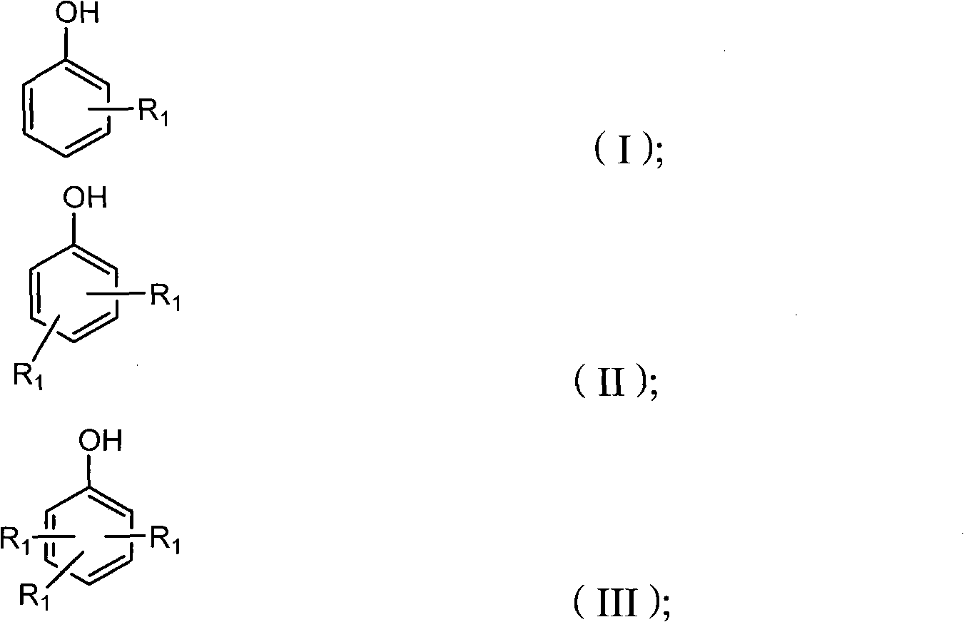
[0099] Add 100 g (0.93 mol) m-cresol, 150 g (1.39 mol) p-cresol, 150 g (37%) formaldehyde to a 1000 ml flask equipped with a heating stirrer, thermometer, reflux condenser and nitrogen inlet and outlet Aqueous solution (1.85 mol) and 3.2 g oxalic acid. Stirring was started and heated to 90-95° C., and the reaction was maintained at this temperature for 3 hours. Then change the reflux device to a simple distillation device, and slowly heat and distill unreacted cresol, formaldehyde and water at atmospheric pressure until 120-130°C. Thereafter, gradually and slowly distill under reduced pressure, so that the vacuum pressure finally reaches 30-60mmHg, the temperature reaches 180°C, stays for 30 minutes, and finally makes the temperature reach 200-220°C in about 15 minutes, and the reaction ends. Stop heating, remove vacuum, put resin into polytetrafluoroethylene or stainless steel dish as soon a...

Embodiment 2

[0103] Embodiment two: a kind of film-forming resin

[0104] (1), phenolic resin

[0105] The solid phenolic resin was prepared according to the same synthesis method as in Example 1. The raw materials are: 150 grams (1.39mol) of m-cresol, 50 grams (0.46mol) of p-cresol, 50 grams (0.46mol) of o-cresol, 150 grams (37%) of formaldehyde solution (1.85mol) and 3.2 grams of oxalic acid . Obtain 220 grams of powdered solid phenolic resin (2), the average molecular weight is 21,000, and the residual phenol in the solid resin is less than 1%.

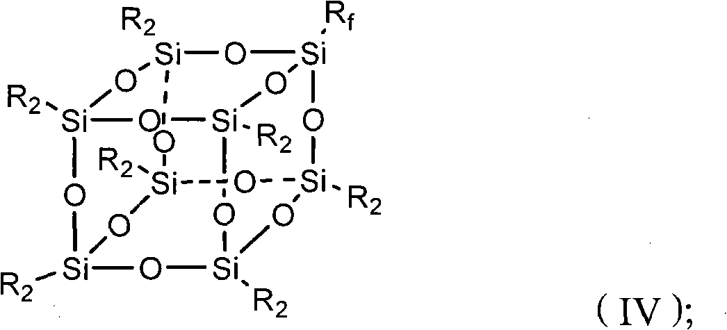
[0106] (2), film-forming resin containing nano-silicon copolymer:

[0107]

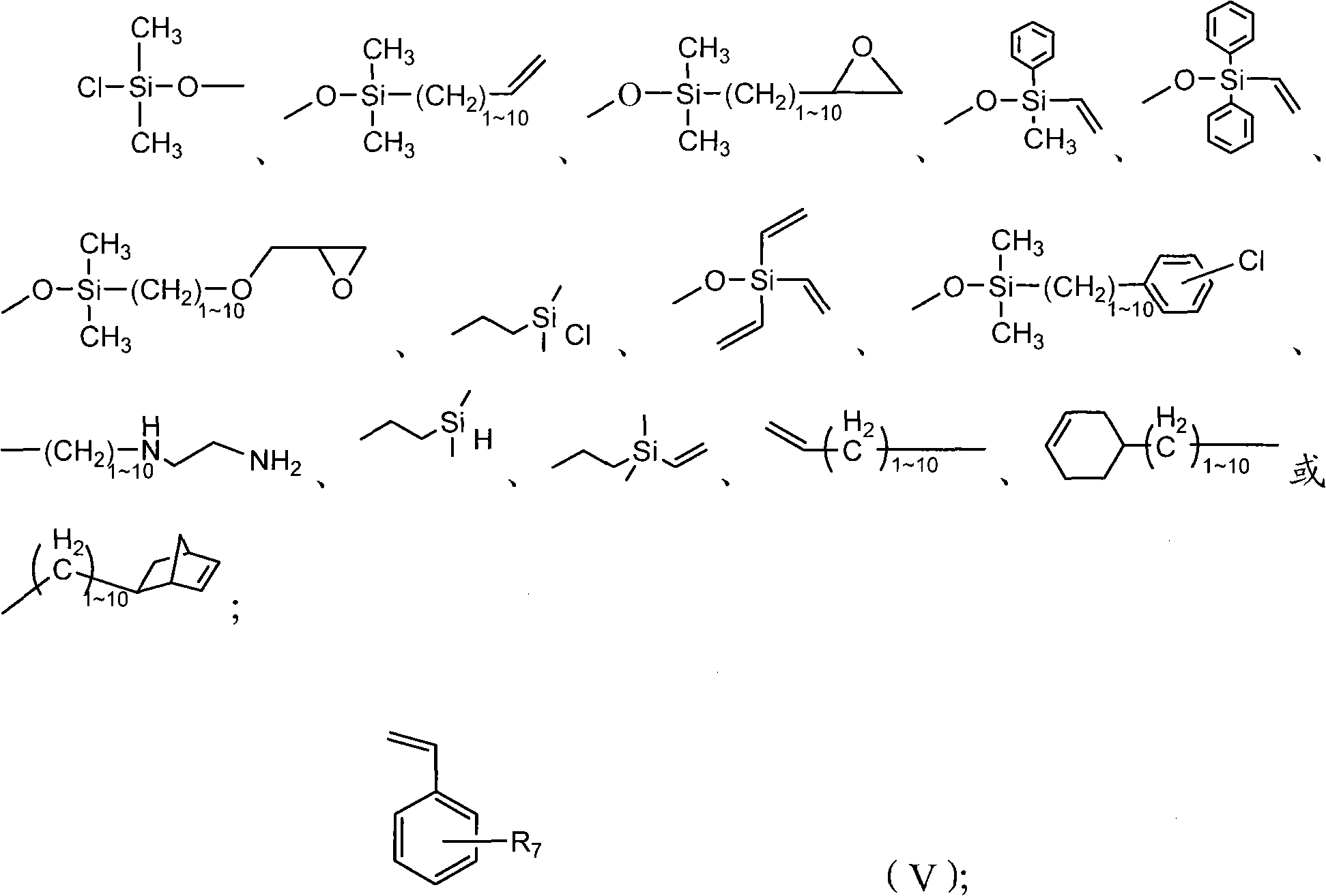
[0108] PF-POSS is prepared by reacting the phenolic resin prepared in this example with polyhedral oligomerized silsesquioxane (POSS):

[0109] Add 50 grams of the cresol-formaldehyde resin prepared in Example 6, 500 grams of solvent PGMEA, and 4 grams of glycidyl POSS in a 1000 milliliter flask equipped with heating stirrer, thermometer, reflux condenser and nitr...

Embodiment 3

[0110] Embodiment three: a kind of film-forming resin

[0111] (1), phenolic resin

[0112] The solid resin was prepared according to the same synthesis method as in Example 1. The raw materials are: 125 grams (1.15mol) of m-cresol, 75 grams (0.69mol) of p-cresol, 50 grams of 3.5-xylenol (0.41mol), 150 grams (37%) of formaldehyde solution (1.85mol) and 3.2 grams of oxalic acid. Obtain 200 grams of powdery solid phenolic resin (3), the average resin molecular weight is 19,000, and the residual phenol in the solid resin is less than 1%.

[0113] Synthesis of polyhedral oligomeric silsesquioxane (POSS)-containing copolymer (P-POSS-B):

[0114] (2), film-forming resin containing nano-silicon copolymer:

[0115]

[0116] 1. Preparation of hydroxystyrene chains:

[0117] Glycidyl methacrylate 272 grams;

[0118] Styrene 11 grams;

[0119] β-Hydroxyethyl Methacrylate 70g

[0120] The preparation method is: in a 1000ml three-necked flask equipped with an electric stirrer, a...


PUM


Abstract

The invention relates to ultraviolet thick film photoresist, which is mainly prepared from 10 to 35 parts of phenolic resin, 1 to 10 parts of nanometer silicon-containing copolymer film forming resin, 5 to 20 parts of diazo naphthoquinone light-sensitive compound, 30 to 85 parts of solvent and a small number of other additives such as n-butylamine and surfactants which serve as raw materials by blending the raw materials and filtering through 5 micrometers, 1 micrometer and 0.2 micrometer filters. The nanometer silicon-containing alkaline soluble copolymer film forming resin is added into the film forming resin to increase the adhesivity, flexibility, side-wall verticality and mechanical properties of a film-forming agent and fulfill the aims of preventing adhesive films from cracking and patterns from deforming and even dropping in a salient point process, three-dimensional (3D) combined encapsulation and the manufacturing of micro-electromechanical systems (MEMS).

Description

technical field [0001] The present invention relates to a kind of ultraviolet thick-film photoresist composition that is applicable to the advanced packaging of large-scale integrated circuit and Micro-Electronic Machine System (MEMS, Micro-Electronic Machine System) etc. film-forming resin. Background technique [0002] In the preparation process of large-scale integrated circuits, advanced packaging technology has developed from individual packaging of a single integrated circuit block to the simultaneous packaging of the entire silicon chip, that is, wafer-level packaging (WLP, waferlevel package), and the packaging of multiple chips Packaging technologies such as stacking and combining into three-dimensional combined packaging with stronger functions have been rapidly promoted, and various packaging materials are required in the packaging process. The thick-film ultraviolet exposure positive photoresist involved in the present invention is a necessary key functional mat...

Claims


Application Information

Patent Timeline
Patent Type & Authority Applications(China)
IPC IPC(8): C08L61/14C08L25/18G03F7/039C08L33/14C08L61/10C08L25/14
Inventor 冉瑞成沈吉
Owner 昆山西迪光电材料有限公司
Why Eureka
Try Eureka