Preparation method for high-density interposer for microelectronic system-in-package

A system-in-package, high-density technology, applied in the process of producing decorative surface effects, microstructure devices, manufacturing microstructure devices, etc. Irregular shape and other problems, to achieve the effects of good thermal stability, low thermal expansion coefficient, and precise adjustable length

Active Publication Date: 2011-05-25
SOUTHEAST UNIV
View PDF2 Cites 21 Cited by
  • Summary
  • Abstract
  • Description
  • Claims
  • Application Information

AI Technical Summary

Problems solved by technology

The DRIE method uses gas to etch the glass, and the etching rate is only 750nm / min. Not only the shape and size of the etched structure are limited, it is impossible to achieve a large aspect ratio, but also the processing efficiency is low and the cost is high.
At present, laser processing is mainly used to prepare through holes, but the cost of laser processing is high, and the shape of the processed holes is irregular. When processing small holes of 3-10 microns, the speed is slower. Metallization by chemical methods is less efficient and more expensive when high-density, small-size lead interconnection is required

Method used


Image

  • Preparation method for high-density interposer for microelectronic system-in-package
  • Preparation method for high-density interposer for microelectronic system-in-package
  • Preparation method for high-density interposer for microelectronic system-in-package

Examples


Embodiment 1

[0030] A method for preparing a high-density adapter board for microelectronic system-in-package, comprising the following steps:

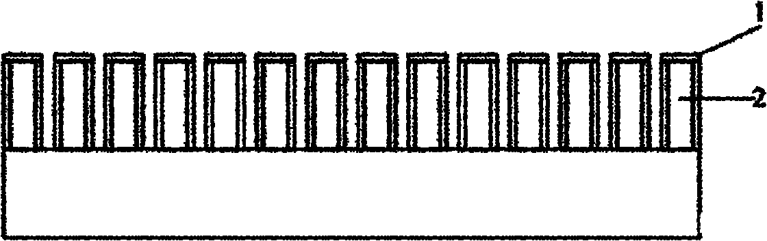
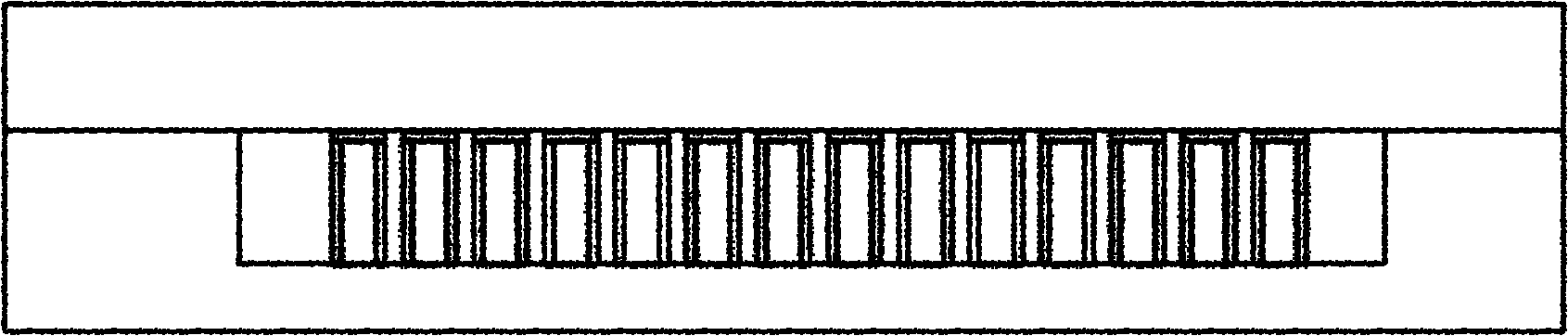
[0031] The first step is to prepare an array 2 of oriented carbon nanotube bundles, the diameter of the carbon nanotube bundles is 0.5-30 microns, such as 0.8 microns, 2 microns, 3 microns, 5 microns, 10 microns, 20 microns, and the spacing is 0.8-100 microns Micron, such as 1 micron, 3 micron, 5 micron, 8 micron, 10 micron, 20 micron, 30 micron, 50 micron, 80 micron, the length is 40-500 micron, such as 45 micron, 60 micron, 100 micron, 200 microns, 300 microns, 400 microns;

[0032] In the second step, metal tungsten 1 is deposited on the surface of the above-mentioned directional growth carbon nanotube bundle to form a conductor array; the thickness of tungsten is 0.1-20 microns, for example, it can be 0.2 microns, 0.8 microns, 1 micron, 5 microns, 10 microns, 15 microns .

[0033] The third step is to make the borosilicate glass and the cond...

Embodiment 2

[0037] A method for preparing a high-density adapter board for microelectronic system-in-package, comprising the following steps:

[0038] The first step is to prepare a directional growth carbon nanotube bundle array, the carbon nanotube bundle has a diameter of 3 microns, a spacing of 5 microns, and a length of 200 microns; the growth method is a plasma-enhanced vapor deposition method, etc.,

[0039] The second step is to deposit metal tungsten on the surface of the above-mentioned carbon nanotube bundle; a layer of tungsten can be prepared on the surface of the carbon nanotube, and the thickness of tungsten is 3 microns. The preparation method can be sputtering, electron beam evaporation or electroplating. , Electron beam evaporation (Ebeam) can make the surface of the carbon nanotube array covered with uniform thickness of tungsten, and has a low surface roughness.

[0040] The third step is to transfer the above-mentioned metallized carbon nanotube bundles into the pre-pre...

Embodiment 3

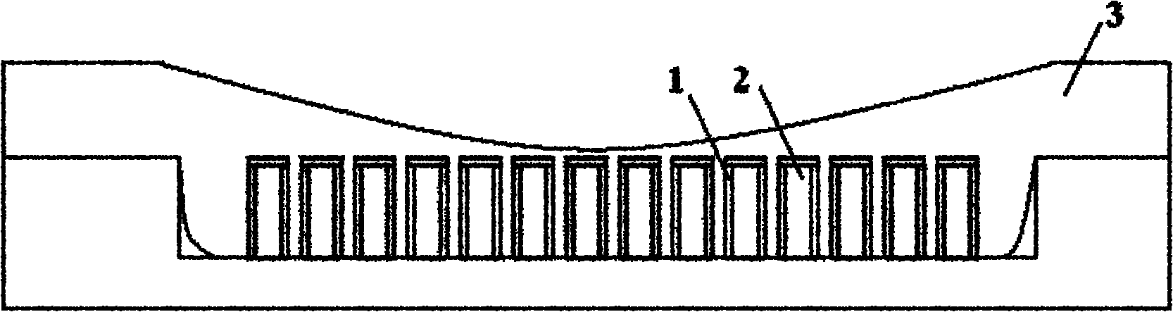
[0045] A method for preparing a high-density adapter plate for microelectronic system-level packaging, comprising the following steps: the first step is to grow a carbon nanotube bundle array on a silicon wafer; the second step is to use the above-mentioned carbon nanotube bundle Array metallization; the third step is to put the above-mentioned metal array into the pre-prepared silicon cavity, and anodically bond the BOROFLOAT33 glass to the silicon cavity; the fourth step is to place the above-mentioned bonded two wafers in the Under one atmospheric pressure, heat the BOROFLOAT33 glass to melt it, make it well combined with the above-mentioned metal array, cool, and anneal the above-mentioned wafer to relieve stress; the fifth step is to remove the silicon for growing carbon nanotubes, and finally A method for preparing a high-density interposer board for microelectronic system-in-package is obtained.

[0046] In the above technical solution, the method for preparing the carb...


PUM

PropertyMeasurementUnit
thicknessaaaaaaaaaa
diameteraaaaaaaaaa
thicknessaaaaaaaaaa

Abstract

The invention discloses a preparation method for a high-density interposer for microelectronic system-in-package. The preparation method comprises the following steps of: 1, preparing a drectionally growing carbon nanotube bundle array, wherein the diameter of each carbon nanotube bundle is 0.5 to 30 microns, the gap of the carbon nanotube bundle is 0.8 to 100 microns, and the carbon nanotube bundle is 40 to 500 microns long; 2, depositing metal tungsten on the surface of the drectionally growing carbon nanotube bundle so as to form a conductor array; 3, melting borosilicate glass and compounding the melted borosilicate glass with the conductor array so as to form a compound body; and 4, grinding the upper surface and the lower surface of the formed compound body so as to expose the end of the carbon nanotube bundle deposited with the metal tungsten, and obtaining the high-density interposer for the system-in-package. The material adopted by the preparation method has low thermal expansivity and the process method is low in time consumption, so the prepared high-density interposer has the advantages of high density, high reliability and low cost.

Description

technical field [0001] The invention relates to a microelectronic manufacturing technology, in particular to a preparation method of a high-density adapter plate used for microelectronic system level packaging. Background technique [0002] In microelectronic systems, the line width on the chip is usually tens of nanometers, while that on the PCB is usually tens to hundreds of microns. Usually, various adapter boards (the interposer in English, including the substrate) are used to interconnect the chip and the PCB board to realize the transition from nanometer to micrometer scale. There are many requirements for the adapter plate, such as low thermal expansion coefficient, high density, high stiffness and low dielectric constant. [0003] The problem with the existing organic material interposer is that it has a high thermal expansion coefficient, a large thermal mismatch with the chip, and its low modulus, which makes the substrate warpage high, so it is difficult to achie...

Claims


Application Information

Patent Timeline
Patent Type & Authority Applications(China)
IPC IPC(8): B81C1/00
Inventor 尚金堂于慧罗新虎蒋明霞刘靖东
Owner SOUTHEAST UNIV
Why Eureka
Try Eureka