Thermal wind sensor based on anodic bonding technology and preparation method thereof

A technology of anodic bonding and wind speed and wind direction, which is applied in the process of producing decorative surface effects, metal material coating process, semiconductor/solid-state device manufacturing, etc., can solve the problem of increasing the sensor, reducing the output sensitive signal amplitude, power consumption Dissipation and other problems to achieve the effect of reducing heat capacity

Inactive Publication Date: 2011-06-01
SOUTHEAST UNIV
View PDF9 Cites 9 Cited by
  • Summary
  • Abstract
  • Description
  • Claims
  • Application Information

AI Technical Summary

Problems solved by technology

As a result, silicon wafers are easily subject to various contaminations, resulting in unstable performance and even damage.
If a ceramic substrate with high thermal conductivity is used, and the silicon chip of the sensor is packaged by flip-chip packaging or thermally conductive adhesive, the above contradictions can be better avoided, but the heat generated by the sensor after packaging is extremely large.

Method used


Image

  • Thermal wind sensor based on anodic bonding technology and preparation method thereof
  • Thermal wind sensor based on anodic bonding technology and preparation method thereof
  • Thermal wind sensor based on anodic bonding technology and preparation method thereof

Examples


Embodiment 1

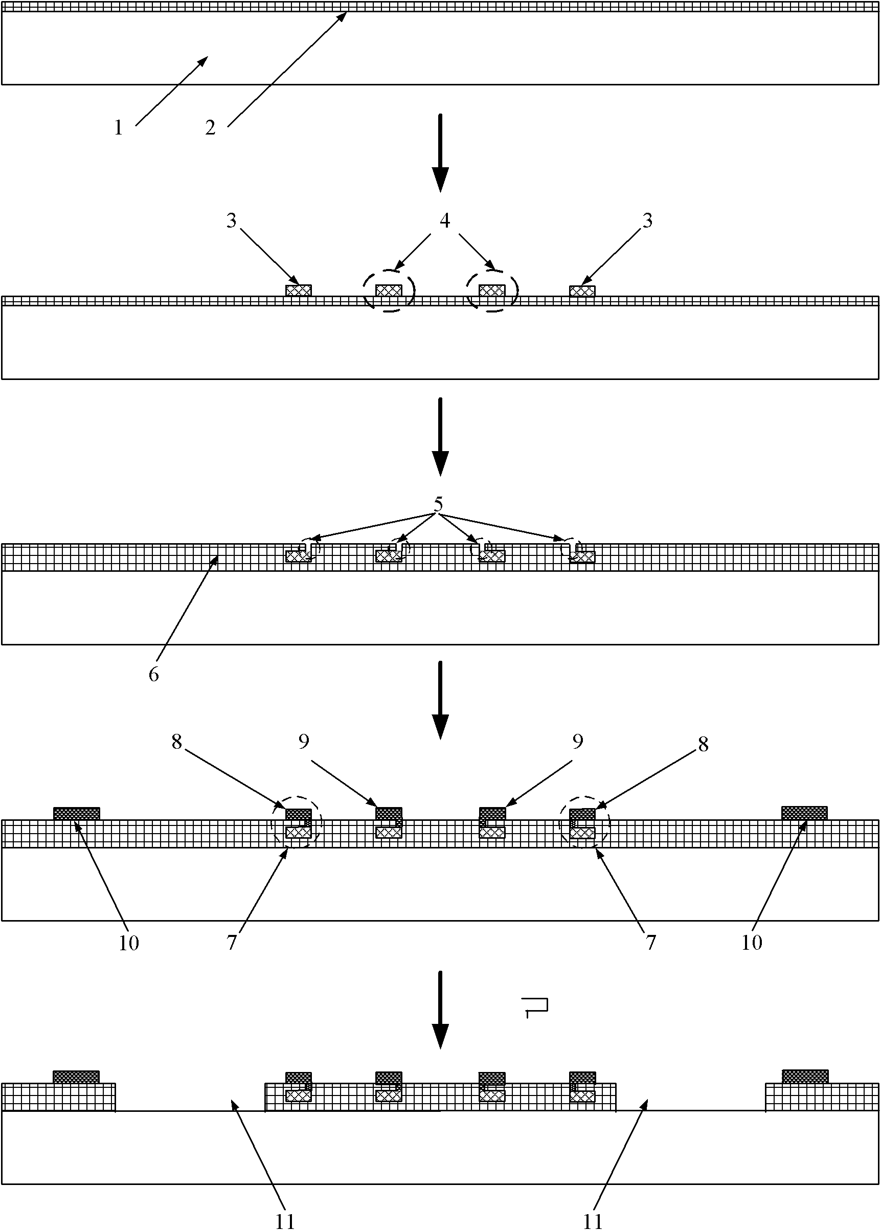
[0039] The manufacturing process of a wafer-level package thermal wind speed and direction sensor based on anodic bonding technology is as follows:

[0040] The first step, the preparation of silicon chips, such as figure 1 shown

[0041] Step 1, thermally growing a first thermal oxide layer 2 on the surface of the silicon chip 1;

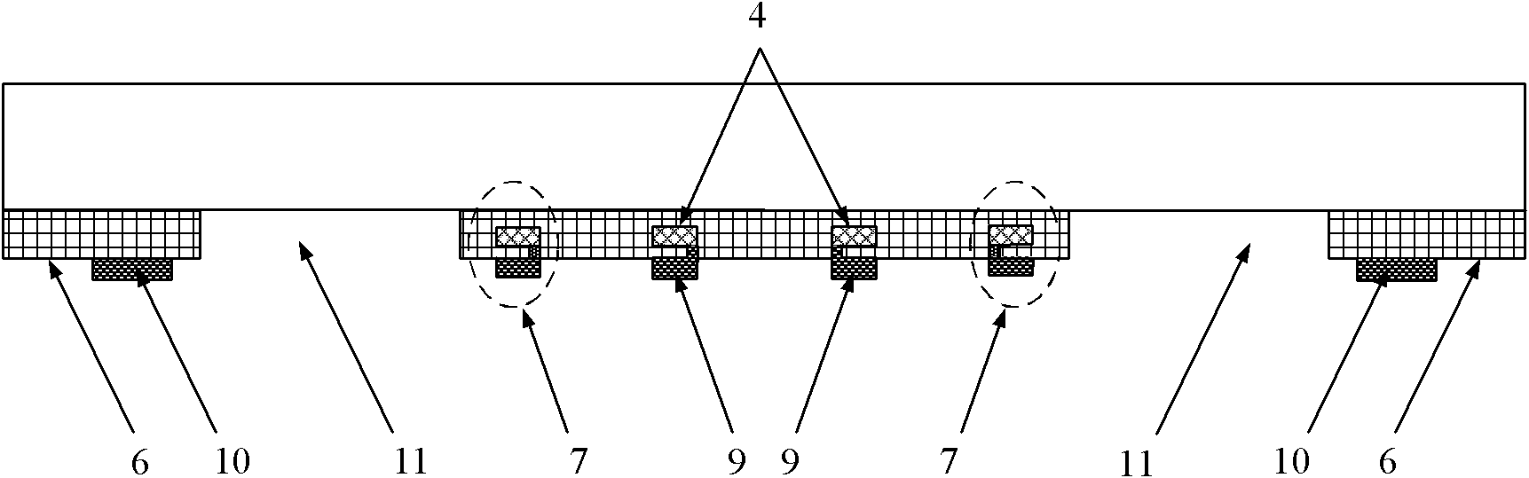
[0042] Step 2, preparing the first polysilicon 3 as one end of the heat sensing temperature measuring element 7 on the first thermal oxide layer 2, and the second polysilicon as the polysilicon heating element 4;

[0043] Step 3, chemical vapor deposition of a second oxide layer on the first thermal oxide layer 2, the first polysilicon 3 and the second polysilicon, and forming an oxide layer 6 from the first thermal oxide layer 2 and the second oxide layer , and use an etching process to etch a through hole 5 on the oxide layer above the first polysilicon 3 and the polysilicon heating element 4;

[0044] Step 4, sputtering and patterning metal a...

Embodiment 2

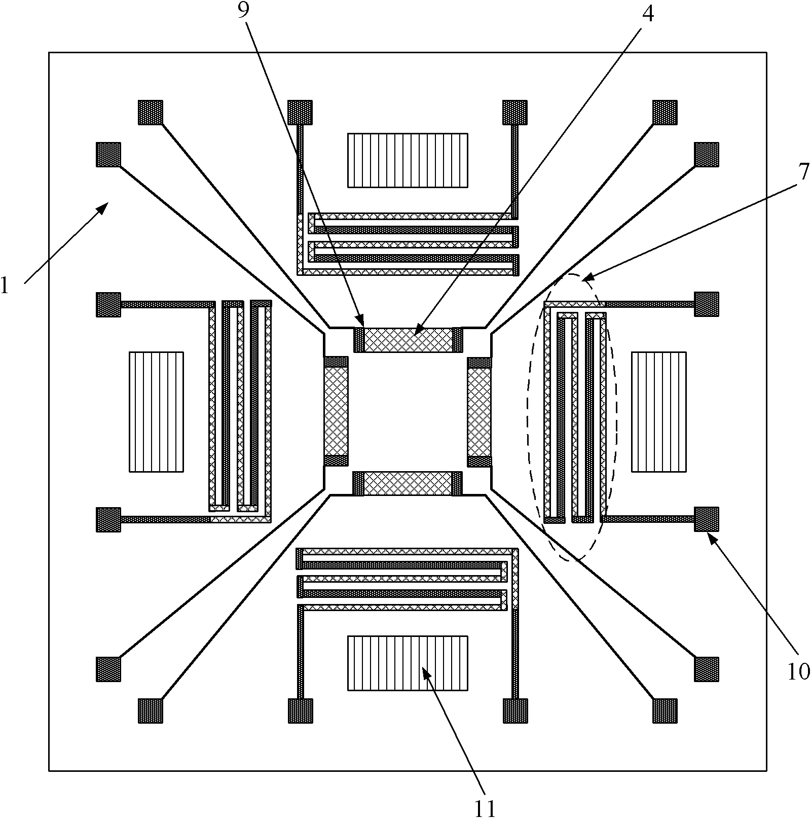
[0058] A thermal wind speed and direction sensor based on the anodic bonding process, comprising a thinned silicon chip 15, the back of the thinned silicon chip 15 is connected with a ceramic sensing substrate 17 through a thermally conductive glue 16, and on the front of the thinned silicon chip 15 An oxide layer 6 is provided, and four polysilicon heating elements 4 and four heat-sensing and temperature-measuring elements 7 are arranged in the middle of the oxide layer 6, and electric lead-out pads 10 are arranged on the edge area of ​​the oxide layer 6, and four polysilicon heating elements are arranged. The element 4 and the four heat-sensing and temperature-measuring elements 7 are respectively connected to the electrical lead-out pad 10 through metal leads. It is characterized in that a bonding cavity 11 capable of exposing a thinned silicon chip 15 is provided on the oxide layer 6. The thinned silicon chip 15 exposed in the bonding cavity 11 is bonded with the packaging ...


PUM


Abstract

The invention discloses a wafer level package thermal wind sensor based on an anodic bonding technology which comprises the following steps: step 1, preparation of silicon chips, manufacturing a heating element, a thermal sensing temperature measuring element and an electric extraction pad by utilizing a standard CMOS (complementary metal-oxide-semiconductor transistor) technology, and etching off an oxide layer at the anodic bonding area at the front surface of the silicon chip by utilizing an MEMS (micro electro mechanical systems) dry etching technology, so that a silicon substrate is exposed; step 2, preparation of packaging glass substrate, preparing bosses for anodic bonding by utilizing an anodic bonding technology, and preparing a through hole for electric extraction by utilizing a laser etching technology; step 3, carrying out bonding packaging on the silicon chips and packaged glass substrate by utilizing the anodic bonding technology; step 4, carrying out thinning on the substrate of the silicon chips by utilizing a thinning technology; step 5, sticking and sealing a ceramic sensing substrate on the back face of the pair of thinned chips; and step 6, scribing and finishing the preparation of the sensor. In the whole preparation process of the sensor, the preparation technologies used are compatible with the standard CMOS technology; the postprocessing technology is simple; the frontage protection of the silicon chips for sensing is realized by the packaging anodic bonding technology; the ceramics are basically sticked and sealed to the back face of the thinned silicon chips, on the one hand, the ceramics serve as heat sensitive materials to sense the wind changes in the outside environment, and on the other hand, the ceramics are used for protecting the silicon chips. By the sensor, the wafer level packaging is realized, and the sensor has the characteristics of good compatibility, simple subsequent technology, and low cost.

Description

technical field [0001] The invention relates to a wafer-level packaged thermal wind speed and direction sensor realized by anodic bonding technology, the preparation process is compatible with the standard CMOS process, in particular to a low power consumption integrated wind speed and direction sensor based on glass and ceramic packaging and its Preparation. Background technique [0002] In the design of CMOS integrated wind speed and direction sensors, packaging has always been a technical bottleneck hindering its development. On the one hand, the encapsulation material is required to have good thermal conductivity and to protect the sensor, and the impact of the encapsulation material on the sensitivity, reliability and price of the sensor needs to be considered in the design, which limits the sensor’s own encapsulation. Design freedom. On the other hand, the thermal flow sensor requires the sensitive part of the sensor to be exposed to the measurement environment, and ...

Claims


Application Information

Patent Timeline
IPC IPC(8): H01L21/60H01L21/8238H01L23/373H01L23/31B81B7/02B81C1/00G01P5/10G01P13/02
CPCH01L2924/0002
Inventor 董自强黄庆安秦明
Owner SOUTHEAST UNIV
Why Eureka
Try Eureka