Groove notching and grid burying method for crystalline silicon solar cell

A technology of solar cells and crystalline silicon, which is applied in the direction of circuits, electrical components, semiconductor devices, etc., can solve the problems of high laser precision, slow speed, and inability to process in batches, and achieve the effect of low fragmentation rate

Inactive Publication Date: 2011-06-01
山东力诺太阳能电力股份有限公司
View PDF4 Cites 13 Cited by
  • Summary
  • Abstract
  • Description
  • Claims
  • Application Information

AI Technical Summary

Problems solved by technology

The disadvantage is that the groove will cause damage to the silicon wafer, cause defects, and affect the efficiency of the cell; after the groove is cut, it must be cleaned to remove the damage
Disadvantages: only single-cut grooving, slow speed, no batch processing, low output; after grooving must be cleaned to remove damage; high precision requirements for laser, more expensive equipment

Method used


Image

  • Groove notching and grid burying method for crystalline silicon solar cell
  • Groove notching and grid burying method for crystalline silicon solar cell

Examples


Embodiment 1

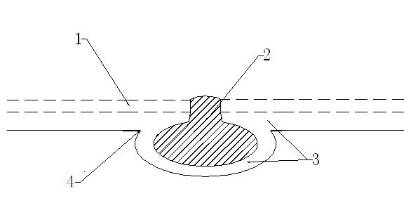
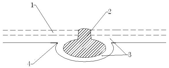
[0028] The polycrystalline silicon wafer 4 is selected; the silicon wafer 4 undergoes a conventional cleaning process, and the surface is textured. At 260°C, a silicon dioxide mask 1 of 80-100nm is deposited on the diffusion surface of the silicon wafer 4 by using the PECVD process, that is, the plasma-enhanced chemical vapor deposition method, and the reaction gas is SiH 4 and O 2 . Print the etching slurry on the electrode 2 on the diffusion surface of the silicon wafer 4 by screen printing. The etching slurry is an organic substance (Merck slurry) containing formic acid and ammonium hydroxide. After etching away the silicon dioxide mask 1 After the silicon wafer 4 is sprayed with pure water, ultrasonically cleaned, ultrasonically cleaned in dilute hydrochloric acid solution, rinsed with circulating pure water, and sprayed with pure water, it is placed in a container containing a 25% nitric acid solution for groove carving. Finally, the remaining impurities and acid soluti...

Embodiment 2

[0030] Example 2: Select a P-type monocrystalline silicon wafer; the silicon wafer undergoes a conventional cleaning process, and the surface is textured, and at a temperature of 400 ° C, 60% of the silicon wafer is deposited on the diffusion surface of the silicon wafer 4 by using the PECVD process, that is, the plasma-enhanced chemical vapor deposition method. ~80nm silicon nitride mask 1, the reaction gas is SiH 4 and NH 3 . Print the etching slurry on the electrode 2 on the diffusion surface of the silicon wafer 4 by screen printing. The etching slurry is an organic substance containing phosphoric acid, and the silicon wafer 4 after the silicon nitride mask 1 has been etched away is sprayed with pure water. , ultrasonic cleaning, ultrasonic cleaning in dilute hydrochloric acid solution, rinsing with circulating pure water, spraying with pure water, put it into a container containing a 15% sodium hydroxide solution for groove carving, and clean the silicon with deionized w...


PUM

PropertyMeasurementUnit
Film thicknessaaaaaaaaaa

Abstract

The invention relates to a groove notching and grid burying method for a crystalline silicon solar cell. The method comprises the following steps of: depositing a mask layer on the surface of a silicon slice, and etching the mask layer at the corresponding electrode position; then notching a groove by a chemical corrosion method to form an electrode groove with a narrow upper part and a wide lower part; and performing screen printing on the electrode groove. The efficiency of the prepared solar cell is improved obviously. The preparation process is simple, resources are saved, and production cost is greatly reduced; damage to a silicon slice and the defect of the silicon slice are avoided by notching the groove by the method, the fragment percent is low, the grooves can be notched on a large scale and the method is suitable for industrial production.

Description

technical field [0001] The invention relates to a method for preparing a solar cell, in particular to a method for carving a groove and burying a gate of a crystalline silicon solar cell. Background technique [0002] Among all kinds of silicon solar cells, crystalline silicon cells have always occupied the most important position. In recent years, great achievements and progress have been made in improving efficiency and reducing costs of crystalline silicon solar cells, further enhancing its advantages in future photovoltaic applications. status. Buried gate battery is one of the most successful examples, it has the prospect of large-scale production, and it is a more practical low-cost and high-efficiency battery technology. Buried gate technology has the advantages of small grid line shadow area, small contact resistance loss, and high current collection efficiency. It is a high-efficiency battery technology that can be industrialized. [0003] At present, there are tw...

Claims


Application Information

Patent Timeline
IPC IPC(8): H01L31/18H01L31/0224
CPCY02P70/50
Inventor 杨青天任现坤刘鹏姜言森李玉花徐振华程亮张春燕王兆光
Owner 山东力诺太阳能电力股份有限公司
Why Eureka
Try Eureka