Low-voltage buried channel VDMOS (vertical double-diffused metal oxide semiconductor) device

A low-voltage, device technology, applied in the field of low-voltage buried trench VDMOS devices, can solve the problem of large reverse leakage current

Inactive Publication Date: 2011-06-15
UNIV OF ELECTRONICS SCI & TECH OF CHINA
View PDF4 Cites 14 Cited by
  • Summary
  • Abstract
  • Description
  • Claims
  • Application Information

AI Technical Summary

Problems solved by technology

However, this structure puts forward higher requirements on the

Method used


Image

  • Low-voltage buried channel VDMOS (vertical double-diffused metal oxide semiconductor) device
  • Low-voltage buried channel VDMOS (vertical double-diffused metal oxide semiconductor) device
  • Low-voltage buried channel VDMOS (vertical double-diffused metal oxide semiconductor) device

Examples


Embodiment Construction

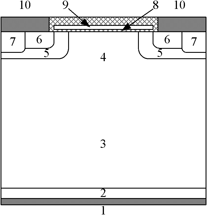
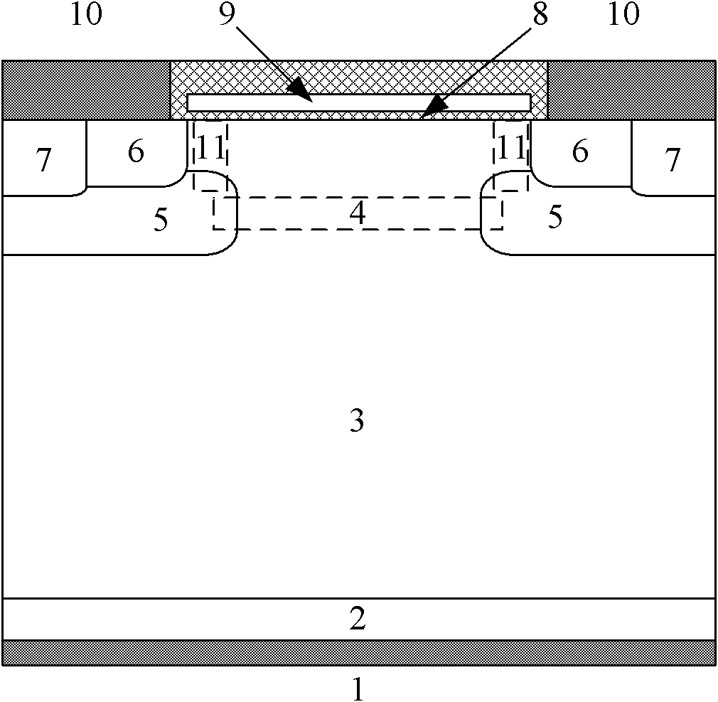
[0025] A low voltage buried trench VDMOS, such as image 3 shown, including metallized cathode 1, N + Substrate Region 2, N - Epitaxial layer 3, JFET region 4, deep P body region 5, P-type heavily doped region 6, N-type heavily doped region 7, gate oxide layer 8, polysilicon gate electrode 9, metalized anode 10, buried Trench structure11.

[0026] A low-voltage buried trench VDMOS device, its embodiment can be prepared by the following method, and the process steps are:

[0027] 1. Preparation of monocrystalline silicon, using N-type heavily doped zone-melted monocrystalline silicon (N-type impurity) substrate 2 with a doping concentration of 1.8×10 19 cm -3 , with a crystal orientation of and a thickness of 5 μm.

[0028] 2. Growth of the epitaxial layer, using the vapor phase epitaxy VPE method to grow 3 μm N on the substrate 2 at a temperature of 1000 ° C and under vacuum conditions. - Epitaxial layer 3, phosphorus doping concentration is 2×10 16 cm -3 .

[0029] ...


PUM

PropertyMeasurementUnit
Thicknessaaaaaaaaaa

Abstract

The invention provides a low-voltage buried channel VDMOS (vertical double-diffused metal oxide semiconductor) device, belonging to the technical field of semiconductor devices. The device has the following beneficial effects: the channel resistance is greatly reduced by adopting the buried layer channel structure; the MOS gate oxide layer is very thin; the MOS surface field effect is utilized; an accumulation layer is formed when forward voltage is applied between the gate and the source while a depletion layer is formed when backward voltage is applied between the gate and the source; and electron or hole accumulation occurs on the lower semiconductor surface of the gate oxide layer under low forward gate voltage, thus acquiring extremely low resistance and good switch characteristics. The device can be widely applied to portable power supplies and CPU power supply systems.

Description

technical field [0001] A low-voltage buried trench VDMOS device belongs to the technical field of semiconductor devices. Background technique [0002] Power MOSFET (Metal Oxide Semiconductor Field Effect Transistor) is a new generation of power switching devices developed on the basis of MOS integrated circuit technology. Vertical double-diffused metal oxide semiconductor (VDMOS) devices have a series of unique features such as high input impedance, fast switching speed, high operating frequency, voltage control, and good thermal stability. Interface circuits and power amplifiers have been widely used. [0003] Although VDMOS (vertical double-diffused metal-oxide-semiconductor field-effect transistor) devices can obtain ideal on-resistance and switching characteristics in low-voltage applications, as the power supply voltage of integrated circuit applications continues to decrease, the on-resistance of power devices The resulting conduction loss has become a bottleneck res...

Claims


Application Information

Patent Timeline
IPC IPC(8): H01L29/78H01L21/265H01L21/336
Inventor 李泽宏姜贯军余士江李婷谢加雄任敏李吉肖璇张波
Owner UNIV OF ELECTRONICS SCI & TECH OF CHINA
Why Eureka
Try Eureka