
Silicon-based Al2O3 film chip capacitor and making method thereof

A thin-film chip and capacitor technology, applied in thin-film/thick-film capacitors, stacked capacitors, fixed capacitor electrodes, etc., can solve the problems of changing chip capacitance height, fixed silicon wafer thickness, poor withstand voltage characteristics, etc., to improve bonding Strength, low cost, good weldability

Active Publication Date: 2013-04-24
SHANGHAI INST OF MICROSYSTEM & INFORMATION TECH CHINESE ACAD OF SCI
View PDF1 Cites 0 Cited by
  • Summary
  • Abstract
  • Description
  • Claims
  • Application Information

AI Technical Summary

Problems solved by technology

However, there are the following problems: 1. The thickness of the silicon wafer is fixed, and the height of the chip capacitance cannot be flexibly changed according to the actual packaging needs; 2. The relative dielectric constant of silicon dioxide is only 3.9, and the dielectric constant k is small, while Al 2 o 3 The relative dielectric constant of ceramics is 9 to 10.5, which is SiO 2 2.5 times that of the same dielectric thickness and capacitance, SiO 2 Film Capacitance Ratio Al 2 o 3 The area of ​​the film capacitor is doubled, and the SiO 2 Breakdown field strength ratio Al 2 o 3 Ceramics are low and have poor withstand voltage characteristics; 3. Using ordinary silicon wafers, the metal back electrode contact will introduce contact resistance, and the silicon wafer itself has a certain resistivity, which will also introduce series parasitic resistance, causing the Q value to drop; 4. Up Electrode, SiO 2 The thin film and Si substrate form a MOS structure. If the doping concentration of the Si substrate is not high enough, no matter it is N-type or P-type, there will be obvious variation characteristics of the capacitance C value with the voltage V. The test C-V curve reflects the obvious electron ( or holes) accumulation and inversion changes, the value of capacitance C changes under positive bias and negative bias conditions, which cannot well meet the needs and applications in actual circuits

Method used


Image

  • Silicon-based Al2O3 film chip capacitor and making method thereof
  • Silicon-based Al2O3 film chip capacitor and making method thereof
  • Silicon-based Al2O3 film chip capacitor and making method thereof

Examples


Embodiment Construction

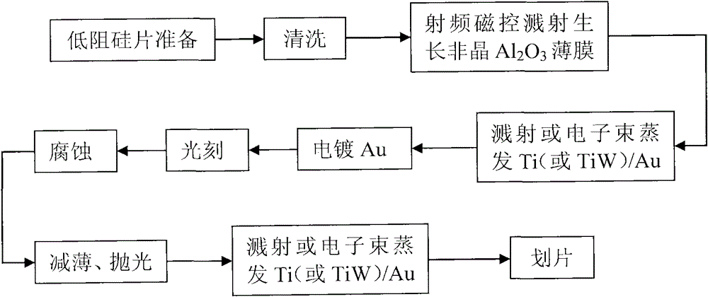
[0026] Below in conjunction with accompanying drawing, describe silicon-based Al of the present invention in detail with embodiment 2 o 3 Structure and characteristics of film chip capacitors. Si-based Al 2 o 3 The thin film chip capacitor and its manufacturing process all belong to the protection scope of the present invention.

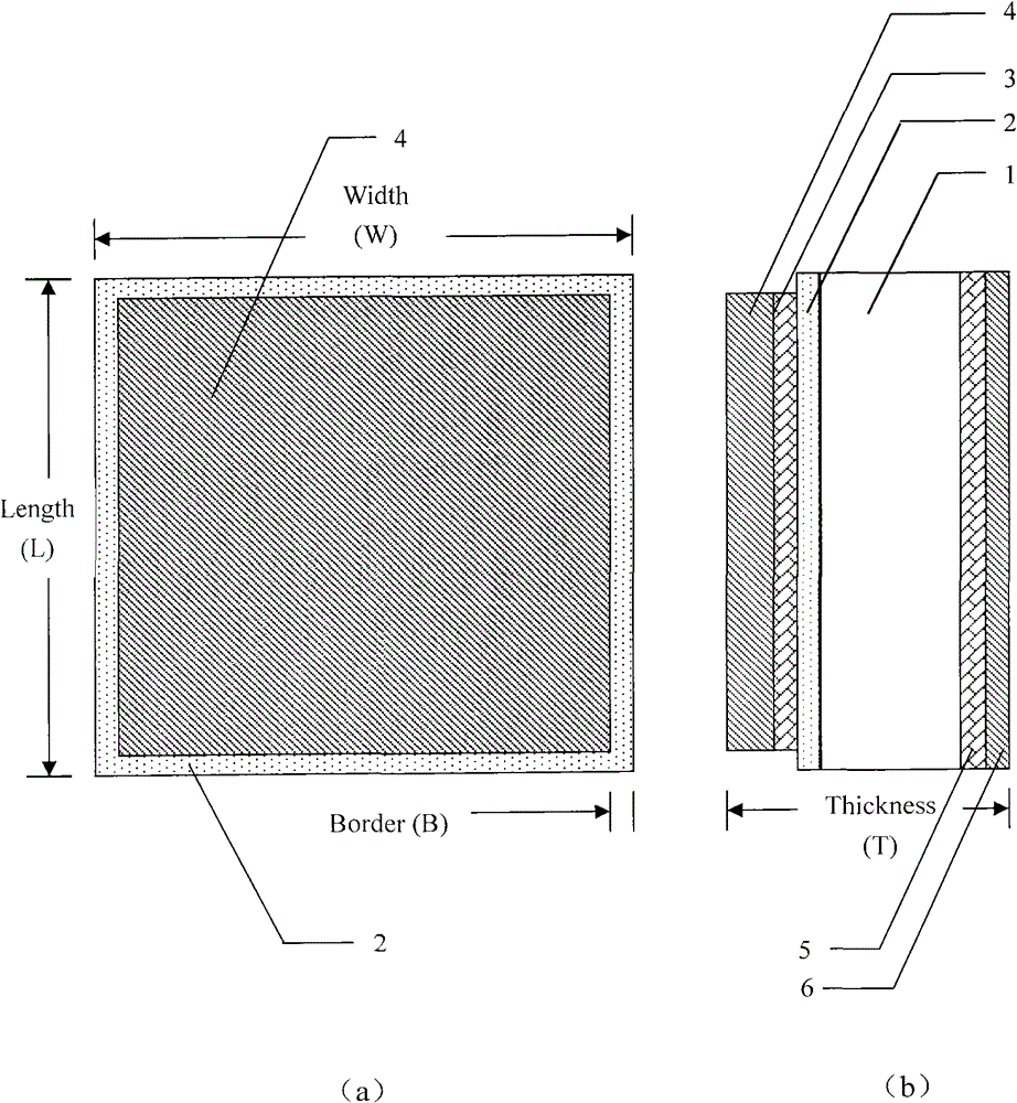
[0027] figure 1 Silicon-based Al showing the present invention 2 o 3 Schematic diagram of the structure of a thin film chip capacitor. Such asfigure 1 (a) As shown in the top view, the edges of the upper electrode Au layer 4 and Ti (or TiW) layer 3 are in contact with Al 2 o 3 A Border (B) region with a width of at least 25 μm is reserved at the edge of the insulating dielectric layer 2 . The edge area B not only improves the breakdown resistance of the edge of the upper electrode plate, but also prevents damage to the insulating medium of the chip capacitor by the scribing process. figure 1 (b) The cross-sectional view more clearly shows t...


PUM

PropertyMeasurementUnit
electrical resistivityaaaaaaaaaa
thicknessaaaaaaaaaa
thicknessaaaaaaaaaa

Abstract

The invention discloses a silicon-based Al2O3 film chip capacitor which can be used for bypass and filtration in microwave and radio-frequency circuits. The chip capacitor comprises a low-resistance (resistivity is not greater than 1*10<-3>omega.cm) silicon substrate, an amorphous Al2O3 insulating film, an upper electrode and a lower electrode. A radio-frequency magnetic control sputtering methodis adopted and comprises the following steps of: growing an amorphous Al2O3 insulating film on a single-crystal Si substrate by using high-purity Al2O3 ceramic as a target material, and then sputtering and growing a Ti or TiW layer and an Au layer; after electroplating Au for thickening, making an upper electrode figure with a photoetching and corroding method; and thinning the back surface of a Si chip according to the requirement on the thickness of the chip capacitor, sputtering the Ti or TiW layer and the Au layer on the back as the lower electrode, and making the chip capacitor after scribing. The capacitor has the advantages of high Q value, low loss, simple structure and process, low cost, small size and the like.

Description

technical field [0001] The invention belongs to the field of film ceramic capacitors, in particular to a microchip capacitor and a manufacturing method. Background technique [0002] Microchip capacitors are a very important electronic device in microwave integrated circuits and multi-chip component packages. They function as bypasses and filters to stabilize the power supply voltage of ICs operating in the microwave frequency band. It is required to be small in size, high in Q value, wide in capacitance value range, and low in cost. [0003] Usually chip capacitors are made by sintering dielectric green sheets and conductor sheets, which have problems such as easy deformation, fragile green porcelain, and special processing for bonding strength. [0004] Another way to make chip capacitors is to use semiconductor technology, which is formed by sequentially forming a lower plate, a dielectric film, and an upper plate on a silicon substrate. This method is suitable for the ...

Claims


Application Information

Patent Timeline
Patent Type & Authority Patents(China)
IPC IPC(8): H01G4/002H01G4/005H01G4/008H01G4/06H01G4/10H01G4/33
Inventor 王伟孙晓玮谈惠祖周健孙浩
Owner SHANGHAI INST OF MICROSYSTEM & INFORMATION TECH CHINESE ACAD OF SCI
Learn More