

Front electrode structure of schottky diode and process manufacturing method of front electrode structure
A technology of Schottky diodes and front electrodes, applied in semiconductor/solid-state device manufacturing, circuits, electrical components, etc., can solve problems such as low packaging yield, device damage, physical characteristics, and electrical characteristics, and achieve anti-ESD Ability improvement and damage reduction effect
- Summary
- Abstract
- Description
- Claims
- Application Information
AI Technical Summary
Problems solved by technology
Method used
Image

Examples
Embodiment Construction
[0034] The entire Schottky diode manufacturing process is further described below in conjunction with the accompanying drawings. As described in the background technology, the front electrode structure of the conventional Schottky diode chip is mostly made of Ti (titanium)-Ni (nickel)-Ag (silver ), V (vanadium)-Ni (nickel)-Ag (silver) and a class of three-layer structure, the realization steps are as follows:
[0035] The voltage divider ring and the main junction of the conventional planar high-voltage transistor are formed at the same time, and the implementation steps are as follows:
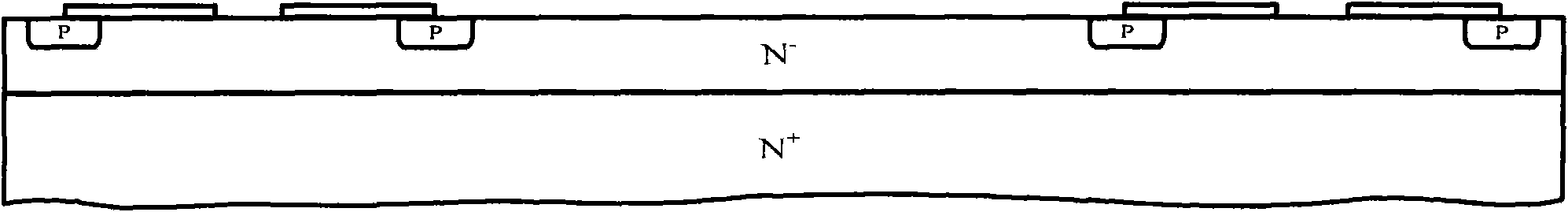
[0036] 1. Clean the Schottky diode chip before vacuum evaporation coating, as shown in Figure 1(a);
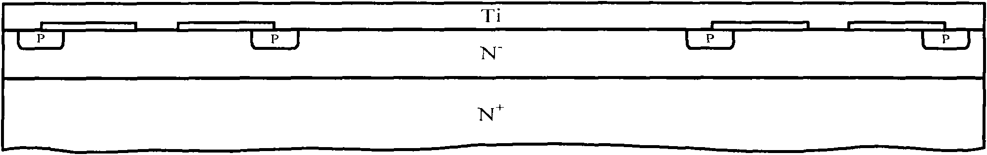
[0037] 2. Vacuum evaporation of metal Ti or V in the contact layer, as shown in Figure 1(b);
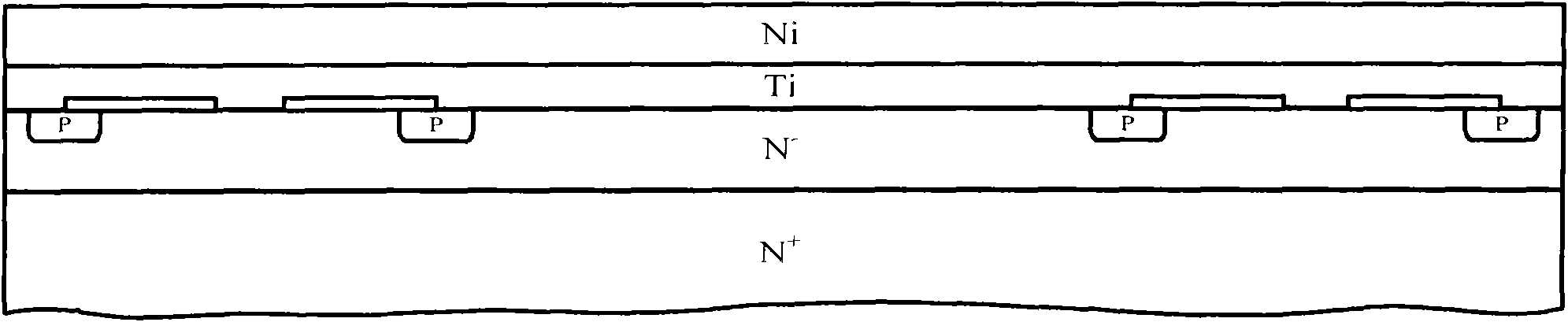
[0038] 3. Vacuum evaporation transition layer metal Ni, as shown in Figure 1(c);
[0039] 4. Vacuum evaporation of conductive layer metal Ag, as shown in Figure 1(d);
[0040] 5. Perform photolit...
PUM
 Abstract
Description
Claims
Application Information