Composite passivated anti-reflection film used for crystalline silicon solar battery and preparation method thereof
A solar cell, crystalline silicon technology, applied in circuits, electrical components, semiconductor devices, etc., can solve the problems of weakening passivation effect, reduced minority carrier life, reduced battery efficiency, etc., and achieves excellent passivation effect, good thermal stability, Good effect of anti-UV performance
- Summary
- Abstract
- Description
- Claims
- Application Information
AI Technical Summary
Problems solved by technology
Method used
Image
Examples
Embodiment 1
[0024] For crystalline silicon solar cells, p-type silicon is the base material, and n+ is the emitter on the light-facing side.
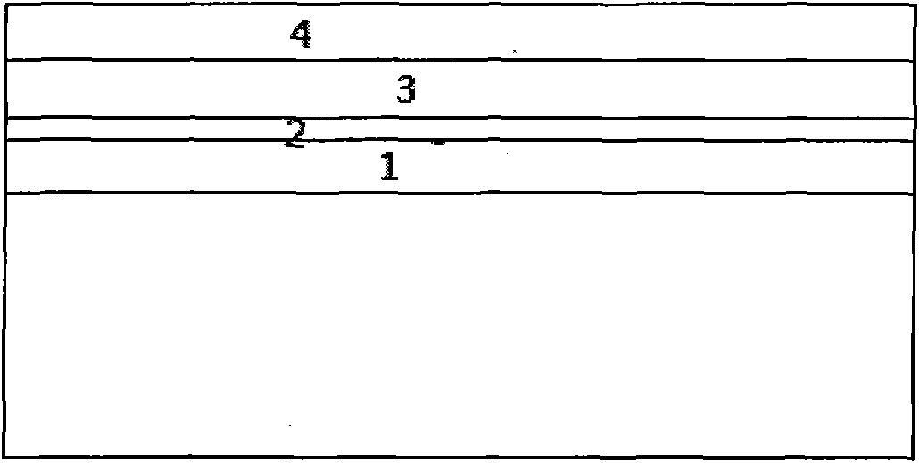
[0025] 1. Quickly soak the surface of the n+ emitter in dilute hydrofluoric acid solution, and then grow a layer of a-Al with a thickness of 5nm by ALD method 2 o 3 Floor;
[0026] 2. Then put the sample in the annealing furnace and anneal in the mixed gas environment of nitrogen and water vapor ratio of 15:1. The annealing temperature is controlled at 500°C, and the annealing time is 30 minutes. 2 o 3 A layer of SiO with a thickness of 1.5nm is automatically generated between the layer and the surface of the n+ emitter 2 Floor;
[0027] 3. Using PECVD method in a-Al 2 o 3 A layer of a-Si with a thickness of 70nm is grown on the 1-X N X film. Among them, the component X=0.57, and the tested refractive index is 2.33.
Embodiment 2
[0029] For crystalline silicon solar cells, p-type silicon is the base material, and n+ is the emitter on the light-facing side.
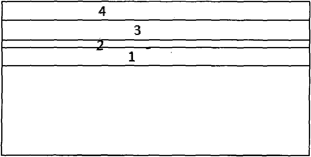
[0030] 1. Quickly soak the surface of the n+ emitter in dilute hydrofluoric acid solution, and then grow a layer of a-Al with a thickness of 20nm by PECVD method 2 o 3 Floor;
[0031] 2. Then put the sample in the annealing furnace, and anneal in the mixed gas environment of nitrogen and water vapor ratio of 15:1, the annealing temperature is controlled at 600°C, the annealing time: 60 minutes, in 2 o 3 A layer of SiO with a thickness of 2nm is automatically generated between the layer and the surface of the n+ emitter 2 Floor;
[0032] 3. Using PECVD method in a-Al 2 o 3 A layer of a-Si with a thickness of 70nm is grown on the 1-X N X film. Among them, the component X=0.57, and the tested refractive index is 2.33.
PUM
| Property | Measurement | Unit |
|---|---|---|
| thickness | aaaaa | aaaaa |
| thickness | aaaaa | aaaaa |
| thickness | aaaaa | aaaaa |
Abstract
Description
Claims
Application Information

