Surface-electrode-technology-based high-throughput cell electrofusion chip device

A surface electrode, high-throughput technology, applied in the field of cell electrofusion, can solve problems such as cell clogging

Inactive Publication Date: 2012-12-05
CHONGQING UNIV
View PDF3 Cites 0 Cited by
  • Summary
  • Abstract
  • Description
  • Claims
  • Application Information

AI Technical Summary

Problems solved by technology

[0022] The purpose of the present invention is to address the deficiencies in the prior art and propose a high-throughput cell electrofusion chip device based on surface electrodes, which integrates an arrayed microelectrode structure on the chip to ensure the integration of microelectrodes and better fusion efficiency , the microelectrode is attached to the polymer microchannel layer, avoiding the problem of cell clogging caused by the traditional tooth-like protruding electrode structure

Method used


Image

  • Surface-electrode-technology-based high-throughput cell electrofusion chip device
  • Surface-electrode-technology-based high-throughput cell electrofusion chip device
  • Surface-electrode-technology-based high-throughput cell electrofusion chip device

Examples


Embodiment 1

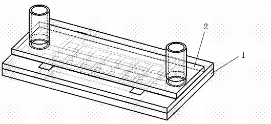
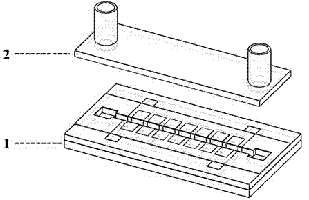
[0041] see figure 1, figure 2 with image 3 , the high-throughput cell electrofusion chip device based on surface electrode technology consists of a high-throughput cell electrofusion chip 1 and a cover sheet 2 with a sample inlet and outlet conduit.

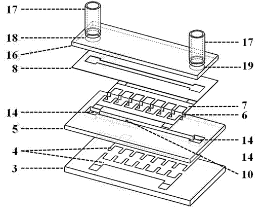
[0042] see image 3 , the high-throughput cell electrofusion chip 1 consists of a quartz base layer 3 , a polymer microchannel layer 5 and a top protective layer 8 from bottom to top.

[0043] Bottom comb-shaped microelectrode array 4, side wall surface electrode layer 6, top comb-shaped micro-electrode array layer 7, which is characterized in that the bottom comb-shaped micro-electrode array layer 4, side wall electrode layer 6 and top comb-shaped micro-electrode array layer 7 Electrically communicated and form a side wall surface electrode array 9 with a “sandwich” structure, combined with the quartz base layer 3 and the polymer microchannel layer 5 to form a smooth flow channel 10 .

[0044] The underlying comb-shaped m...

Embodiment 2

[0051] Embodiment 2: the using method of this device

[0052] In the experiment, a micropump can be used to inject the cell suspension into the chip from the injection port 18 in Example 1. When the cell suspension flows through the microchannel 10, a sine wave electrical stimulation signal is loaded through the bonding point 13 or 15, A non-uniform gradient electric field will be formed between the microelectrodes on the opposite side walls, and the two cells between the microelectrodes will line up under the action of dielectrophoretic force. After the queuing is completed, a square wave pulse sequence signal is applied, and the queuing cell pairs will complete the process of cell electroporation-cell electrofusion under the action of a high-intensity pulse electric field between the microelectrodes. After the cell electrofusion process is completed, the micropump is used to inject the cell culture solution, and the cells in the microchannel flow out through the microchann...

Embodiment 3

[0053] Example 3: Fabrication of high-throughput cell electrofusion chip device

[0054] Using MEMS processing technology, the processing technology is as follows:

[0055] A. Clean the quartz glass sheet;

[0056] B. Put the quartz glass sheet in the evaporation furnace, and evaporate and deposit to form 2000 the gold film;

[0057] C. Spin-coat AZ4620 on the surface of the gold film, and form the same pattern as the underlying microelectrode array structure after exposure and development;

[0058] D. Place the quartz glass sheet in gold etching solution and HF etching solution successively to remove excess gold film and form the underlying microelectrode array structure;

[0059] E. Acetone removes the residual AZ4620 on the surface of the underlying microelectrode array structure;

[0060] F. cleaning;

[0061] G. Spin-coat PI7510 on the surface of the quartz glass sheet, expose and develop to form a polymer microchannel layer, and place it in a curing oven to cure PI...


PUM

PropertyMeasurementUnit
thicknessaaaaaaaaaa
thicknessaaaaaaaaaa
widthaaaaaaaaaa

Abstract

The invention relates to a surface-electrode-technology-based high-throughput cell electrofusion chip device. The device consists of a microelectrode array chip and a cover plate with a sample charging and discharging guide pipe, wherein the microelectrode array chip comprises a quartz basal layer, a polymer microchannel layer and a top protective layer from bottom to top in turn; a bottom comb-shaped microelectrode array is manufactured on the quartz basal layer; the middle of the polymer microchannel layer is provided with a microchannel; a top comb-shaped microelectrode array of which the shape and the position correspond to those of the bottom comb-shaped microelectrode array is manufactured on the polymer microchannel layer; the side wall of the microchannel is provided with a side wall surface electrode; and the side wall surface electrode is connected with each pair of comb teeth corresponding to the bottom comb-shaped microelectrode array and the top comb-shaped microelectrodearray, so that the side wall surface and the top and bottom comb-shaped microelectrode arrays are electrically communicated to form a sandwich structure. The microelectrode arrays are attached to thepolymer microchannel layer, so that the problem of cell blockage caused by the conventional toothed protruding electrode structure is solved, and the integration level and high fusion efficiency of microelectrodes are ensured simultaneously.

Description

technical field [0001] The present invention relates to cell electrofusion technology, in particular to a high-throughput cell electrofusion chip device based on surface electrodes. In the research of transfection, it can be widely used in genetics, animal and plant distant hybrid breeding, developmental biology, drug screening, monoclonal antibody preparation, mammalian cloning and other fields. Background technique [0002] Since the 1980s, cell electrofusion technology has been rapidly developed and widely used because of its high efficiency, simple operation, non-toxicity to cells, easy observation, suitable for instrument application and standardized operation. [0003] Cell electrofusion can be divided into two main stages: cell queuing and cell fusion. [0004] The principle of cell queuing is that when biological cells are in a non-uniform electric field, they are polarized by the electric field to form a dipole, and the dipole will move under the action of a specif...

Claims


Application Information

Patent Timeline
Patent Type & Authority Patents(China)
IPC IPC(8): C12M1/42C12N15/02
CPCC12M35/02
Inventor 胡宁杨军郑小林罗洪艳廖彦剑侯文生许莎张小玲刘琳琳胡晋豪徐涛
Owner CHONGQING UNIV
Why Eureka
Try Eureka