Method for manufacturing gallium nitride-based LED (Light Emitting Diode) with vertical structure

A gallium nitride-based, vertical structure technology, applied in electrical components, circuits, semiconductor devices, etc., can solve the problems of reduced chip yield, easy generation of bubbles in wafers, and reduced reliability, achieving a small difference in thermal expansion coefficients and improving thermal conductivity. performance, the effect of improving yield

Inactive Publication Date: 2011-09-14
TONGHUI ELECTRONICS
View PDF2 Cites 6 Cited by
  • Summary
  • Abstract
  • Description
  • Claims
  • Application Information

AI Technical Summary

Problems solved by technology

Due to the whole chip bonding (bonding), air bubbles are likely to be generated between the two bonded chips, resulting in weak local bonding, which reduces the yield and reliability of the subsequent chips;
[0007] ③The size of the transfer substrate should not be too large (generally round, with a diameter of less than 100 cm), and cannot be made into shapes other than round

Method used


Image

  • Method for manufacturing gallium nitride-based LED (Light Emitting Diode) with vertical structure
  • Method for manufacturing gallium nitride-based LED (Light Emitting Diode) with vertical structure
  • Method for manufacturing gallium nitride-based LED (Light Emitting Diode) with vertical structure

Examples


Embodiment 1

[0029] ① Preparation of LED chips

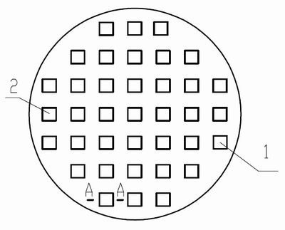
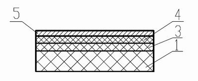
[0030] On the sapphire substrate 1, the n-type GaN layer 3 and the p-type GaN layer 4 are epitaxially sequentially, and the mutually independent LED chips 2 are formed on the sapphire substrate 1 through a photolithography process, see figure 1 ; Evaporate metal ITO, NiAg or NiAu on the surface of the LED chip 2, and treat it in a nitrogen atmosphere at 200-400°C for 1-10min to form a p-electrode 5; then thin the sapphire substrate 1: use diamond-containing Grinding with a grinding wheel, then polishing with a polishing solution containing diamond sand, and thinning the sapphire substrate 1 to 70-120 μm; finally, cutting the sapphire substrate according to the LED chip 2 into individual pieces independently by cutting with a laser, a diamond knife or a grinding wheel saw The LED chip, the cross-sectional schematic diagram of a single LED chip see figure 2 .

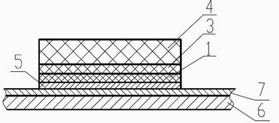
[0031] ② Treatment of composite metal substrates

[0032] A gold layer 7 is eva...


PUM

PropertyMeasurementUnit
thicknessaaaaaaaaaa
diameteraaaaaaaaaa

Abstract

The invention discloses a method for manufacturing a gallium nitride-based LED (Light Emitting Diode) with a vertical structure. The method comprises the following steps of: (1) extending an n-type semiconductor layer and a p-type semiconductor layer on a sapphire substrate in sequence to form an LED wafer, performing metal evaporation on the surface of the LED wafer and treating in a nitrogen atmosphere at the temperature between 200 DEG C and 400 DEG C for 1-10 minutes to form a p electrode, and partitioning the LED wafer into independent LED chips; (2) evaporating gold layers on the upper surface and the lower surface of a composite metal substrate respectively, wherein the composite metal substrate is made of a copper-molybdenum alloy or an aluminum-silicon alloy; (3) reversely welding the independent LED chips obtained in the step (1) onto the upper surface of the composite metal substrate respectively; (4) stripping substrates of the LED chips; and (5) manufacturing an n-type electrode on an n-type semiconductor material of each LED chip. In the method, a CuMo or AlSi composite metal substrate with high thermal conductivity is taken as a transfer substrate and has a small thermal expansion coefficient difference from a transferred LED chip, the thermal stress is small, and the bonding yield is increased.

Description

technical field [0001] The invention relates to a method for preparing an LED, in particular to a method for preparing a gallium nitride-based LED with a vertical structure. Background technique [0002] China is currently one of the countries with the fastest urbanization process in the world. It can be expected that in the next few decades, the market demand for high-power, high-brightness, and energy-saving LED street lamps across the country will be extremely huge. According to the statistics of the national street lamp industry, there are more than 15 million street lamps for urban road lighting in my country, and the growth rate in recent years has been more than 20%. According to this estimate, the annual market size of lighting street lamps in the country is not less than 5 billion yuan. If LED street lamps are used, more than 2 billion kWh of electricity can be saved every year. One of the core technologies of LED street lamps is the blue light high-power LED chip....

Claims


Application Information

Patent Timeline
Patent Type & Authority Applications(China)
IPC IPC(8): H01L33/00
Inventor 李云王静辉任继民苏银涛肖国华徐海洲李兴
Owner TONGHUI ELECTRONICS
Why Eureka
Try Eureka