A multilayer back reflector structure for thin film solar cells
A technology of solar cells and mirrors, applied in the fields of circuits, electrical components, sustainable manufacturing/processing, etc., can solve the problems of no explanation or report, and data not yet collected, etc., to improve photoelectric conversion efficiency, high yield, Improve the effect of short-circuit current
- Summary
- Abstract
- Description
- Claims
- Application Information
AI Technical Summary
Problems solved by technology
Method used
Image
Examples
Embodiment 1
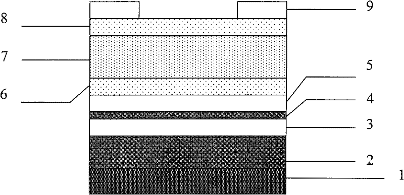
[0024] With flexible stainless steel with a thickness of 50 μm as the substrate 1, two back reflector structures were prepared by magnetron sputtering (working frequency: 13.56 MHz): the back reflector (1) was Ag with a thickness of 500 nm deposited sequentially on the substrate. Membrane, the ZnO of 100nm: Al thin film; Back reflector (2) is the Ag film 2, the ZnO of 100nm: Al thin film 3, the Ag thin film 4 of 10nm, the ZnO of 100nm: Al thin film that deposit thickness is 500nm on the substrate successively 5.
[0025] Using the plasma-assisted chemical vapor deposition method (PECVD, the operating frequency is 13.56MHz), on the flexible stainless steel substrate (used to prepare sample 1), the prepared back reflector (1) (used to prepare sample 2), the back reflector Deposit identical N, I, P three-layer silicon film on mirror (2) (for preparing sample three); Wherein N layer reaction gas is hydrogen, silane, phosphine, thickness is about 50nm; I layer reaction gas is hydro...
Embodiment 2
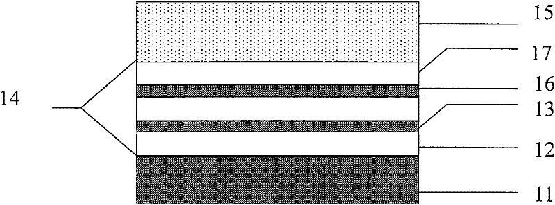
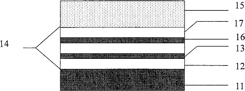
[0030] The multilayer back reflector structure is prepared by electron beam evaporation method: the multilayer back reflector structure is to deposit Ag film 11 with a thickness of 1000nm and SnO with a thickness of 500nm on the substrate. 2 : F oxide transparent conductive film 12, 20nm Ag film 13, 500nm SnO 2 : F conductive film, 20nm Ag thin film 16, 500nm SnO 2 : F conductive film 17. The multi-layer back reflector can be applied to thin-film solar cells whose absorption layers are made of amorphous silicon, microcrystalline silicon, nano-silicon, amorphous silicon germanium, copper indium gallium selenide, and cadmium telluride [15]. Various types of tandem solar cells. structured as figure 2 shown.
Embodiment 3
[0032] Using 50 μm thick flexible stainless steel as the substrate, the multilayer back reflector structure was prepared by vacuum thermal evaporation method: the multilayer back reflector structure is to deposit Al film with a thickness of 200nm on the substrate, and ZnO:Ga oxide with a thickness of 200nm Transparent conductive film, 3nm Al film, 200nm ZnO:Ga conductive film, 3nm Al thin film, 200nm ZnO:Ga conductive film, 3nm Al thin film, 200nm ZnO:Ga conductive film.
[0033] Using the plasma-assisted chemical vapor deposition method (PECVD, the working frequency is 13.56MHz), on the prepared multi-layer back reflector structure, deposit N, I, P three-layer silicon film: the reaction gas of the N layer is hydrogen, silane , Phosphine, the thickness is about 50nm; I layer reaction gas is hydrogen, silane, thickness is about 300nm; P layer reaction gas is hydrogen, silane, borane, methane, thickness is about 30nm.
[0034] A magnetron sputtering method (operating frequency o...
PUM
 Abstract
Description
Claims
Application Information


