Electrophoresis cell with conductive diamond film as electrode
A technology of conductive diamond and diamond film, which is applied in the direction of material analysis, instruments, and measuring devices by electromagnetic means, to achieve the effects of wide potential window, easy cleaning, uniform strength and gradient distribution
- Summary
- Abstract
- Description
- Claims
- Application Information
AI Technical Summary
Problems solved by technology
Method used
Image
Examples
Embodiment 1
[0022] Embodiment 1: The overall structure of the electrophoresis tank of the present invention
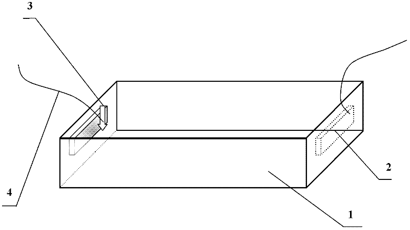
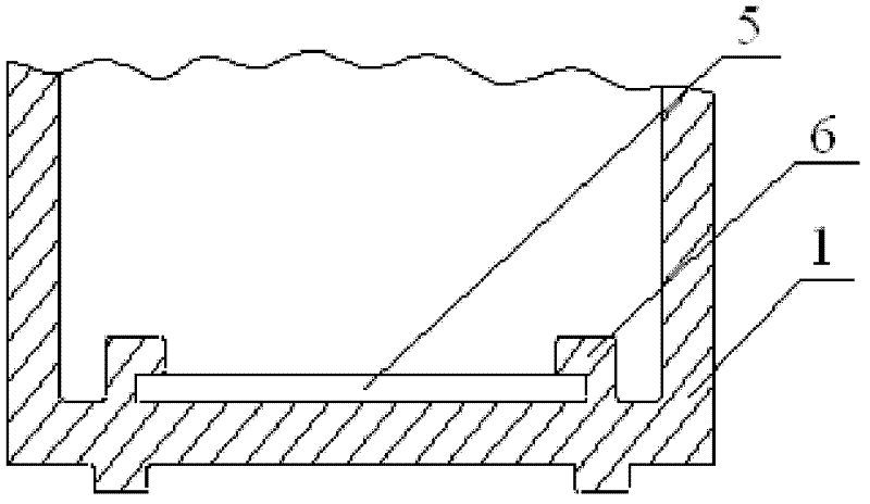
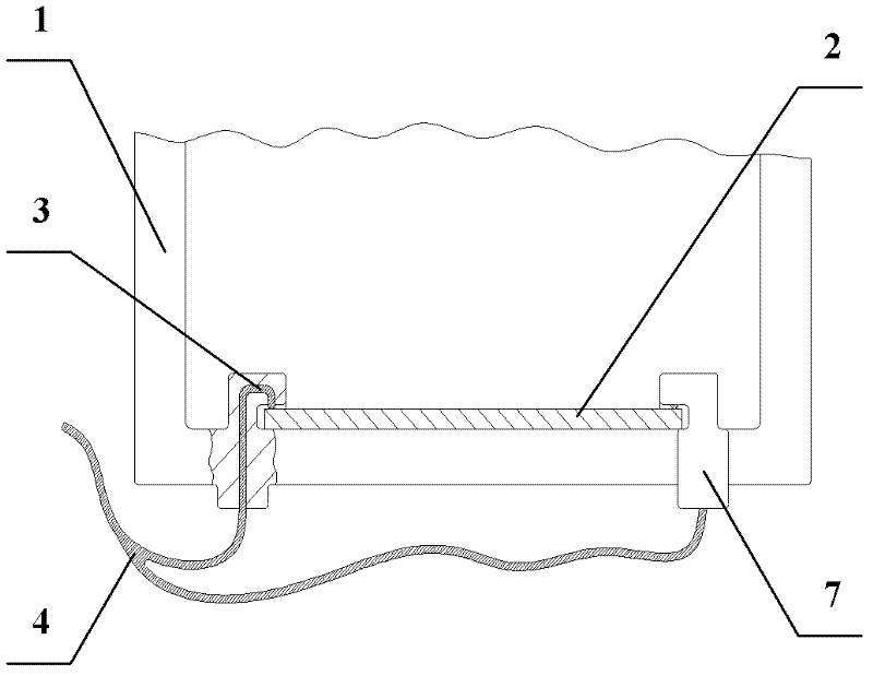
[0023] The overall structure of the electrophoresis tank of the present invention is as follows Figure 1 ~ Figure 3 shown. Figure 1~3 Among them, 1 is the electrophoresis tank; 2 is the conductive diamond film electrode, which is a rectangular electrode with a thickness of about 5 μm to 2000 μm; 3 is the electrode fixing device (for the specific structure of the fixed slot electrode fixing device, refer to figure 2 ); 4 is the wire, connects the power supply and the electrode, and the position where the wire is connected to the electrode is as the criterion so that the wire does not contact the buffered conductive solution; The width of the electrode 2 is adapted so that the conductive diamond film electrode 2 slides down along the two grooves 6 and is stuck in the groove 6; 5 is the lower supporting plate of the electrode fixing device, and when the conductive diamond film el...
Embodiment 2
[0024] Embodiment 2: the making of the conductive diamond film electrode of boron doping
[0025] In the first step, p-type diamond is grown, that is, a boron-doped p-type CVD polycrystalline diamond film is grown. Microwave plasma chemical vapor deposition (MWCVD), hot filament chemical vapor deposition (HFCVD), DC hot cathode CVD or DC jet CVD can be used, using borane or trimethyl borate as boron source; Different substrates (such as silicon, silicon carbide and various industrial electrode materials - molybdenum, niobium, tantalum, titanium, tungsten, zirconium and graphite, etc.) grow boron-doped diamond films.
[0026] The parameters of the growth conditions of the conductive diamond film are listed as one of the methods-microwave plasma CVD method: the substrate is p-type Si, the microwave power is 300-1000W, the pressure is 7-8kPa, the flow rate of hydrogen gas is 200-300sccm, and the flow rate of methane gas is 4 ~6 sccm, boron source uses borane or trimethyl borate,...
Embodiment 3
[0030] Embodiment 3: the making of conductive diamond film electrode doped with nitrogen
[0031] The substrate Si used in the present invention is an n-type (111) single crystal silicon wafer with a thickness of 0.5mm. Using microwave plasma CVD deposition, the experimental gas for preparing conductive diamond film electrodes is H 2 / CH 4 / N 2 , the gas ratio is 110 / 10 / 30sccm. The input power and reaction pressure were 250W and 50Torr, respectively. Deposition time 4h. The resistivity of the thus prepared conductive diamond film is in the range of 10 -3 Ω·cm level.
PUM
| Property | Measurement | Unit |
|---|---|---|
| electrical resistivity | aaaaa | aaaaa |
| thickness | aaaaa | aaaaa |
| electrical resistivity | aaaaa | aaaaa |
Abstract
Description
Claims
Application Information


