A kind of preparation method of single crystal graphene
A single crystal graphene, graphene technology, applied in the direction of single crystal growth, single crystal growth, chemical instruments and methods, etc., can solve the problems affecting the electrical properties of graphene film, small crystal domains of graphene film, difficult to control, etc. To achieve the effect of research and application promotion, simple method and low cost
- Summary
- Abstract
- Description
- Claims
- Application Information
AI Technical Summary
Problems solved by technology
Method used
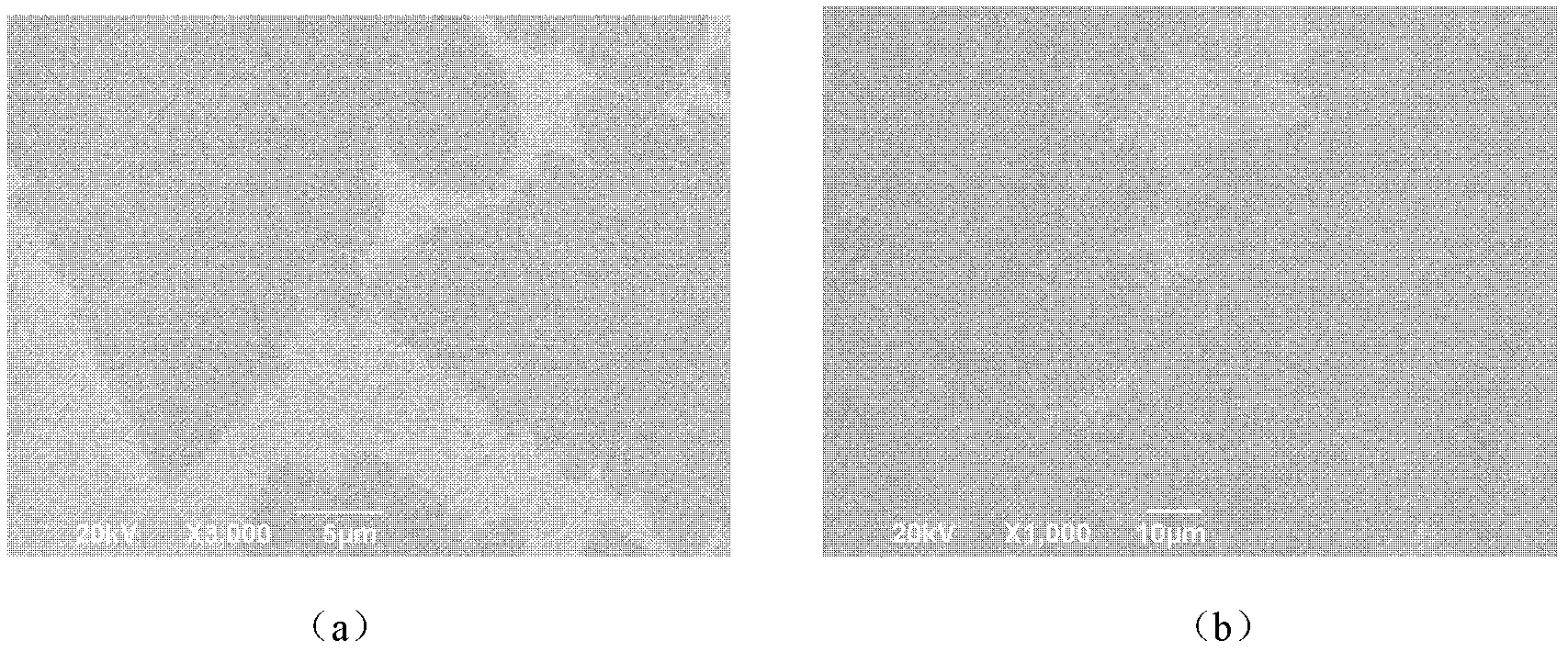
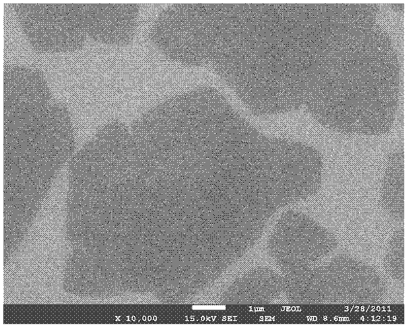
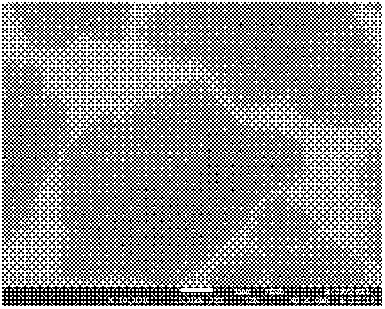
Image

Examples
Embodiment 1
[0019] Embodiment 1, adopt PMMA powder to prepare single crystal graphene on copper foil, its concrete steps are as follows:
[0020] Fold the 5 cm x 5 cm metal copper foil in half, put 1g of PMMA powder into it, then seal it up, place it in a chemical vapor deposition chamber and feed 10SCCM (30Pa) of hydrogen and 500SCCM (200Pa) of argon at 25°C / The speed was raised to 1000°C for 80 minutes, and then lowered to room temperature at a speed of 50°C / min to obtain single crystal single atomic layer graphene on the outside of the metal copper foil.
[0021] The single crystal single atomic layer graphene obtained by this embodiment has a ratio of G peak intensity to 2D peak intensity of 0.3, no defect D peak, and a mobility of 16000 cm 2 / Vs.
Embodiment 2
[0022] Embodiment 2, adopt imidazole powder to prepare single crystal nitrogen-doped graphene on nickel foil, its specific steps are as follows:
[0023] Fold a 5 cm x 5 cm metal nickel foil in half, put 0.5 g of imidazole powder into it, then seal it up, place it in a chemical vapor deposition chamber and feed 50 SCCM (80 Pa) of hydrogen and 1000 SCCM (500 Pa) of argon at 25 ° C The speed is raised to 900°C / min, maintained for 150 minutes, and then lowered to room temperature at a speed of 100°C / min, and single crystal nitrogen-doped graphene is obtained on the outside of the metal nickel foil.
[0024] The monocrystalline nitrogen-doped graphene obtained by this example has a ratio of G peak intensity to 2D peak intensity of 1, a defect D peak to G peak ratio of 0.01, a nitrogen atom content of 2%, and a mobility of 500 cm 2 / Vs.
Embodiment 3
[0025] Embodiment 3, using tripropyl boron powder to prepare single crystal boron-doped graphene on nickel foil, its specific steps are as follows:
[0026] Fold a 10 cm x 10 cm metal nickel foil in half, put 2g of tripropyl boron powder into it, then seal it, place it in a chemical vapor deposition chamber and feed 50SCCM (80Pa) of hydrogen and 800SCCM (300Pa) of argon to The temperature was raised to 1020 °C at a rate of 25 °C / min, maintained for 180 minutes, and then lowered to room temperature at a rate of 250 °C / min to obtain single crystal boron-doped graphene on the outside of the metal nickel foil.
[0027] The monocrystalline boron-doped graphene obtained by this example has a ratio of G peak intensity to 2D peak intensity of 1.2, a defect D peak to G peak ratio of 0.05, a boron atomic content of 1%, and a mobility of 300 cm 2 / Vs.
PUM
| Property | Measurement | Unit |
|---|---|---|
| thickness | aaaaa | aaaaa |
Abstract
Description
Claims
Application Information
 - R&D
- Intellectual Property
- Life Sciences
- Materials
- Tech Scout
- Unparalleled Data Quality
- Higher Quality Content
- 60% Fewer Hallucinations
Browse by: Latest US Patents, China's latest patents, Technical Efficacy Thesaurus, Application Domain, Technology Topic, Popular Technical Reports.
© 2025 PatSnap. All rights reserved.Legal|Privacy policy|Modern Slavery Act Transparency Statement|Sitemap|About US| Contact US: help@patsnap.com