Organic electronic device

A technology of organic electronic devices and devices, applied in the direction of electric solid devices, electrical components, organic chemistry, etc., can solve problems such as voltage increase, high voltage, and shortened life

Active Publication Date: 2012-01-11
MERCK PATENT GMBH
View PDF105 Cites 15 Cited by
  • Summary
  • Abstract
  • Description
  • Claims
  • Application Information

AI Technical Summary

Problems solved by technology

In particular, the properties of these materials are often also limiting for the lifetime, efficiency and operating voltage of organic electroluminescent devices.
[0004] QUR 3 have been used as electron transport materials for some time (e.g. US 4,539,507), but AlQ 3 Has a number of disadvantages: it cannot be vapor deposited without residues, since at sublimation temperatures it partially decomposes, which represents a major problem especially for production plants
The result of this is that the vapor deposition source has to be cleaned or replaced repeatedly
In addition, AlQ 3 The decomposition products reach the OLED, where they cause shortened lifetime and reduced quantum and power efficiencies
In addition, AlQ 3 Has low electron mobility, which leads to higher voltage and thus lower power efficiency
In order to avoid short circuits in the display, it is desirable to increase the thickness of the layer; for AlQ 3 This is not possible due to the low charge carrier mobility and the resulting voltage increase
The charge-carrier mobility of other electron conductors (US 4,539,507) is also too low to construct thicker layers with them, where the lifetime of the OLED is even longer than when using AlQ 3 worse
QUR 3 The intrinsic color (yellow in the solid state) of 2000 has also proven to be unfavorable, possibly causing a color shift due to reabsorption and weak re-emission, especially in the case of blue OLEDs

Method used


Image

  • Organic electronic device
  • Organic electronic device
  • Organic electronic device

Examples


Embodiment 1

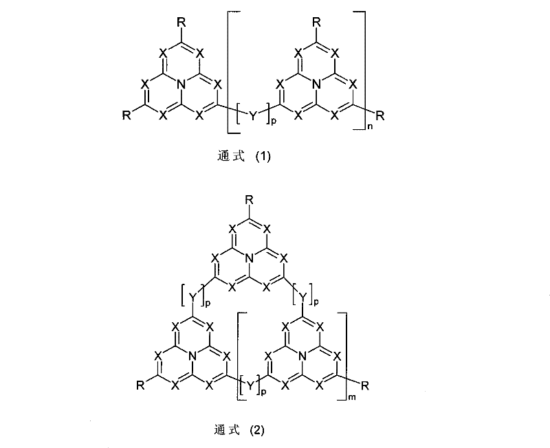
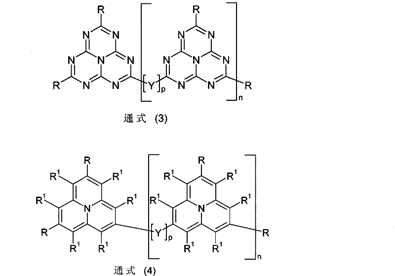
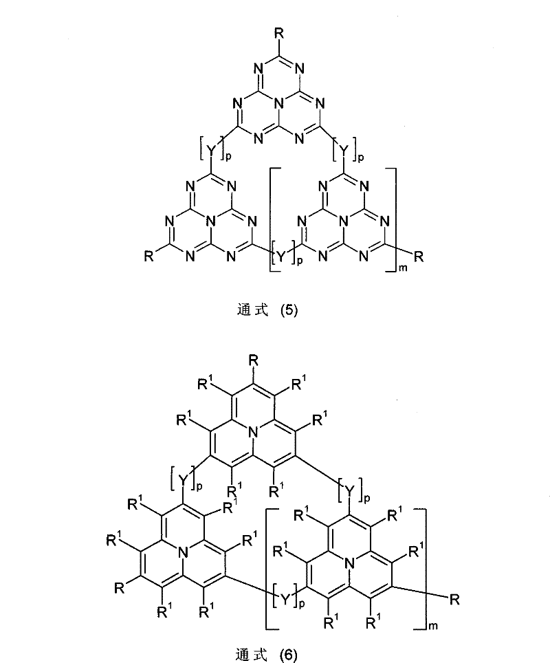
[0104] Example 1: Synthesis of Tricyanoheptaazaphenene (HIM-1)

[0105]

[0106] 50 g (181 mmol) of trichloroheptaazafinene and 53.45 g (597 mmol, 3.3 equivalents) of copper (I) cyanide were suspended in 750 ml of DMF and heated at 130° C. for 60 h under argon. After cooling to room temperature, the reaction mixture was added to 1000 ml of concentrated ammonia solution and vigorously stirred in the air for 4 h. The organic precipitate precipitated in the process was filtered with suction and washed with cold ethanol. The residue was extracted with acetonitrile in a Soxhlet extractor, and the crystalline precipitate was filtered off with suction, washed with a little cold acetonitrile and dried under vacuum. Yield: 39.1 g (157 mmol), 87% of theory; purity is about 99.8% (HPLC).

Embodiment 2

[0107] Example 2: Manufacturing and characterization of organic electroluminescent devices

[0108] The OLED of the invention is manufactured by a general method according to WO 04 / 058911, which method has to be adapted to the situation described here (layer-thickness variation, material used).

[0109] In the following Examples 3 to 8, the results of various OLEDs are provided. A glass plate coated with structured ITO (Indium Tin Oxide) forms the base of the OLED. For improved processing, 20nm PEDOT (spin-coated from water; purchased from HCStarck, Goslar, Germany; poly(3,4-ethylenedioxy-2,5-thiophene)) was applied to the substrate on. The OLED consists of the following layer sequence: substrate / PEDOT 20nm / hole injection layer (HIL) 5nm / hole transport layer (HTM-1) 20nm / hole transport layer (HTL-2) 20nm / light emitting layer (EML) 30nm / Electron transport layer (ETM) 20nm and the final cathode.

[0110] The material except PEDOT is applied by thermal vapor deposition in a vacuum ...


PUM

PropertyMeasurementUnit
glass transition temperatureaaaaaaaaaa
thicknessaaaaaaaaaa

Abstract

The present invention relates to organic electroluminescent devices comprising aromatic nitrogen heterocyclics, in particular in a hole injection layer and / or in a hole blocking layer and / or in an electron transport layer and / or in an emitting layer.

Description

Technical field [0001] The present invention relates to an organic electronic device including an aromatic nitrogen-containing heterocyclic compound, especially an organic electroluminescent device. Background technique [0002] For example, in US 4539507, US 5151629, EP 0676461 and WO 98 / 27136, the structure of an organic electroluminescent device (OLED) in which organic semiconductors are used as functional materials is described. However, before these devices can be used in high-quality and long-life displays, it is still hoped that they will be further improved. Therefore, there is still a need for improvement, especially in terms of the life, efficiency and operating voltage of organic electroluminescent devices. In addition, it is necessary for the compound to have high thermal stability and be able to sublime without decomposition. [0003] In particular, it is still desired to improve charge injection materials and charge transport materials, because it is the properties ...

Claims


Application Information

Patent Timeline
Patent Type & Authority Applications(China)
IPC IPC(8): C09K11/06
CPCC09K11/06C09B3/22C09B57/00H01L51/0072C09B1/00C09K2211/1081C09K2211/1074C09K2211/1029C09K2211/1466H05B33/14C09B57/008C09K2211/1491Y02E10/549C09K2211/1483C09K2211/1475C09B3/02C07D221/14C07D259/00H10K85/6572H10K50/16H10K50/17
Inventor 埃斯特·布罗伊宁
Owner MERCK PATENT GMBH
Why Eureka
Try Eureka