Method for preparing diamond-graphene composite film
A graphene composite and diamond technology, applied in metal material coating process, gaseous chemical plating, coating, etc., can solve the problems that single diamond film cannot meet, and achieve environmental protection, good reliability, unique and singular performance effect
- Summary
- Abstract
- Description
- Claims
- Application Information
AI Technical Summary
Problems solved by technology
Method used
Image
Examples
Embodiment 1
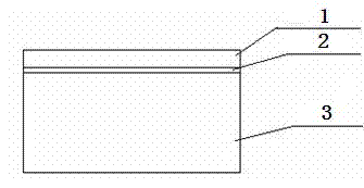
[0026] Such as figure 1 As shown, diamond powder with a particle size of 800nm, 200nm, 50nm, and 20nm is used to impact and etch the growth surface of the substrate at a high speed of 100-500m / s on the ground Ni substrate 3 to obtain high surface energy and high Micro-nano pits on the surface of the density substrate, and then ultrasonically clean and purify the surface of the substrate for 20 minutes, then put it into the growth chamber, vacuumize and clean the growth chamber, start the DC plasma arc, and then introduce high-concentration active hydrogen atoms to the surface of the planar nickel substrate The micro-nano pits are further subjected to reactive etching, so that the substrate forms high surface energy micro-nano pits with a specific structure, forming nucleation centers, and inducing the nucleation and growth of graphene 2.
[0027] A direct current plasma jet chemical vapor deposition system is used, and then the nickel substrate is placed on a special cooling t...
Embodiment 2
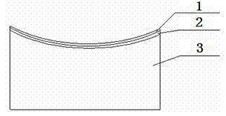
[0030] As shown in Figure 2, cubic boron nitride with a particle size of 10 μm, 1 μm, 100 nm, and 10 nm is used to impact and etch the concave surface substrate 3 at a high speed of 150-450 m / s on the ground Ni substrate 3. To grow the surface, obtain micro-nano pits on the surface of the substrate with high surface energy and high density, and then perform 25 minutes of ultrasonic cleaning on the surface of the substrate 3, then put it into the growth chamber, vacuumize and clean the growth chamber with argon gas, and then start the DC plasma arc , and then introduce high-concentration active hydrogen atoms to further reactively etch the micro-nano pits on the surface of the concave curved nickel substrate, so that the substrate forms micro-nano pits with a specific structure and high surface energy, and induces the nucleation and growth of graphene 2.
[0031]A direct current plasma jet chemical vapor deposition system is used, and then the nickel substrate is placed on a spe...
Embodiment 3
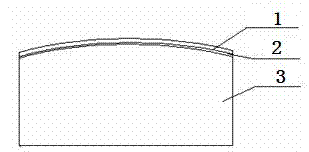
[0034] Such as image 3 As shown, diamond powder with a particle size of 5 μm, 500 nm, 200 nm, and 50 nm is used to impact and etch the growth surface of the convex curved substrate 3 at a high speed of 80-600 m / s on the ground Ni substrate 3 to obtain a high surface area. High-energy, high-density substrate surface with micro-nano pits, and then ultrasonically clean and purify the surface of the convex curved substrate 3 for 30 minutes, then put it into the growth chamber, vacuumize and clean the growth chamber, start the DC plasma arc, and then introduce high-concentration active hydrogen Atoms further reactively etched the micro-nano pits on the surface of the convex curved nickel substrate, so that the substrate formed micro-nano pits with a specific structure and high surface energy, which induced the nucleation and growth of graphene.
[0035] A direct current plasma jet chemical vapor deposition system is used, and then the convex curved nickel substrate is placed on a ...
PUM
| Property | Measurement | Unit |
|---|---|---|
| thickness | aaaaa | aaaaa |
| particle diameter | aaaaa | aaaaa |
| particle diameter | aaaaa | aaaaa |
Abstract
Description
Claims
Application Information


