Porous nickel-copper oxide nanowire array enzyme-free glucose sensor electrode on titanium substrate
A glucose sensor and porous nanowire technology, applied in the field of enzyme-free glucose sensor electrodes, can solve the problems of expensive glucose oxidase, poor electrochemical performance, and difficult storage, and achieve the effects of low cost, fast response, and low limit
- Summary
- Abstract
- Description
- Claims
- Application Information
AI Technical Summary
Problems solved by technology
Method used
Image
Examples
Embodiment 1
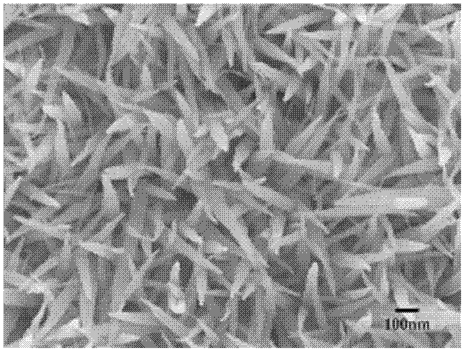
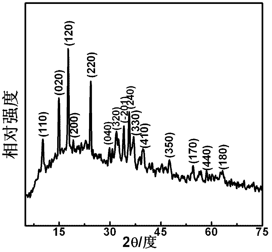
[0034] Precursor (Ni, Cu) 2 (OH) 2 CO 3 Preparation of nanowire arrays: clean titanium metal sheet (3×2×0.03cm 3 ) into 0.32 grams of copper chloride dihydrate (CuCl 2 2H 2 O), 0.24 grams of nickel chloride hexahydrate (NiCl 2 ·6H 2 O) and 0.7 gram of urea in 80 milliliters of aqueous solutions; Then seal and heat to 120 ℃ in the autoclave of polytetrafluoroethylene liner, keep 24 hours; After natural cooling, titanium metal sheet is taken out, obtains the precursor of electrode sample (Ni, Cu) 2 (OH) 2 CO 3 Nanowire Array Films. The samples were observed by scanning electron microscope and X-ray diffraction. The results show that the precursor (Ni, Cu) 2 (OH) 2 CO 3 The nanowires are distributed vertically, uniformly and densely on the surface of the titanium metal sheet, presenting a nanowire array structure. The diameter of the top of a single nanowire is 20 nanometers, and the length is 2 microns. The results are shown in figure 1 and figure 2 .
Embodiment 2
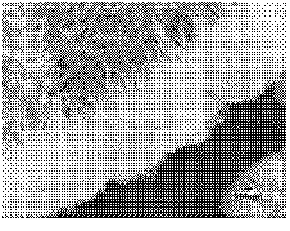
[0036] The precursor (Ni, Cu) on the titanium substrate 2 (OH) 2 CO 3 The nanowire array film was placed in a box furnace at 350° C. for 60 minutes and annealed to obtain a porous nanowire array film with NiO / CuO nanoparticles cross-assembled on the titanium substrate. Then the morphology and crystal structure of the samples were observed by scanning electron microscope, transmission electron microscope and X-ray diffractometer. The result is expressed in image 3 , Figure 4 and Figure 5 middle. It can be seen from the figure that the nanowire array basically maintains the state before annealing, but the single nanowire has become a porous structure. The nanowires are cross-assembled by NiO and CuO nanoparticles, and the size of the nanoparticles and nanopores are both 5 nm. The X-ray diffraction results of the samples annealed at 350℃ show that the annealing temperature is lower and the crystallization state of the samples is poor.
Embodiment 3
[0038] The precursor (Ni, Cu) on the titanium substrate 2 (OH) 2 CO 3 The nanowire array film was annealed in a box furnace at 500°C for 60 minutes to obtain a porous nanowire array film with cross-assembled NiO and CuO nanoparticles on the titanium substrate. Then the morphology and crystal structure of the samples were observed by scanning electron microscope, transmission electron microscope and X-ray diffractometer. The result is expressed in Figure 6 , Figure 7 and Figure 8 middle. It can be seen from the figure that the nanowire array basically maintains the state before annealing, but the single nanowire has become a porous structure. The nanowires are cross-assembled by NiO and CuO nanoparticles, and the size of the nanoparticles and nanopores are both 5 nm. The X-ray diffraction results of the samples annealed at 500°C show that the higher the annealing temperature, the better the crystalline state of the samples.
PUM
| Property | Measurement | Unit |
|---|---|---|
| diameter | aaaaa | aaaaa |
| length | aaaaa | aaaaa |
| Sensitivity | aaaaa | aaaaa |
Abstract
Description
Claims
Application Information


