Lateral double-diffusion metal oxide semiconductor (LDMOS) device introducing local stress

A local stress and device technology, applied in semiconductor devices, electrical components, circuits, etc., can solve problems such as unfavorable device drive capabilities, and achieve the effects of improving device drive capabilities, high withstand voltage characteristics, and reducing adverse effects

Active Publication Date: 2012-07-04
UNIV OF ELECTRONICS SCI & TECH OF CHINA
View PDF5 Cites 2 Cited by
  • Summary
  • Abstract
  • Description
  • Claims
  • Application Information

AI Technical Summary

Problems solved by technology

The length and concentration of the drift region affect the LDMOS breakdown voltage and the source-drain on-resistance R on The two important factors of the drift region, the longer the length of the drif

Method used


Image

  • Lateral double-diffusion metal oxide semiconductor (LDMOS) device introducing local stress
  • Lateral double-diffusion metal oxide semiconductor (LDMOS) device introducing local stress
  • Lateral double-diffusion metal oxide semiconductor (LDMOS) device introducing local stress

Examples


Embodiment 1

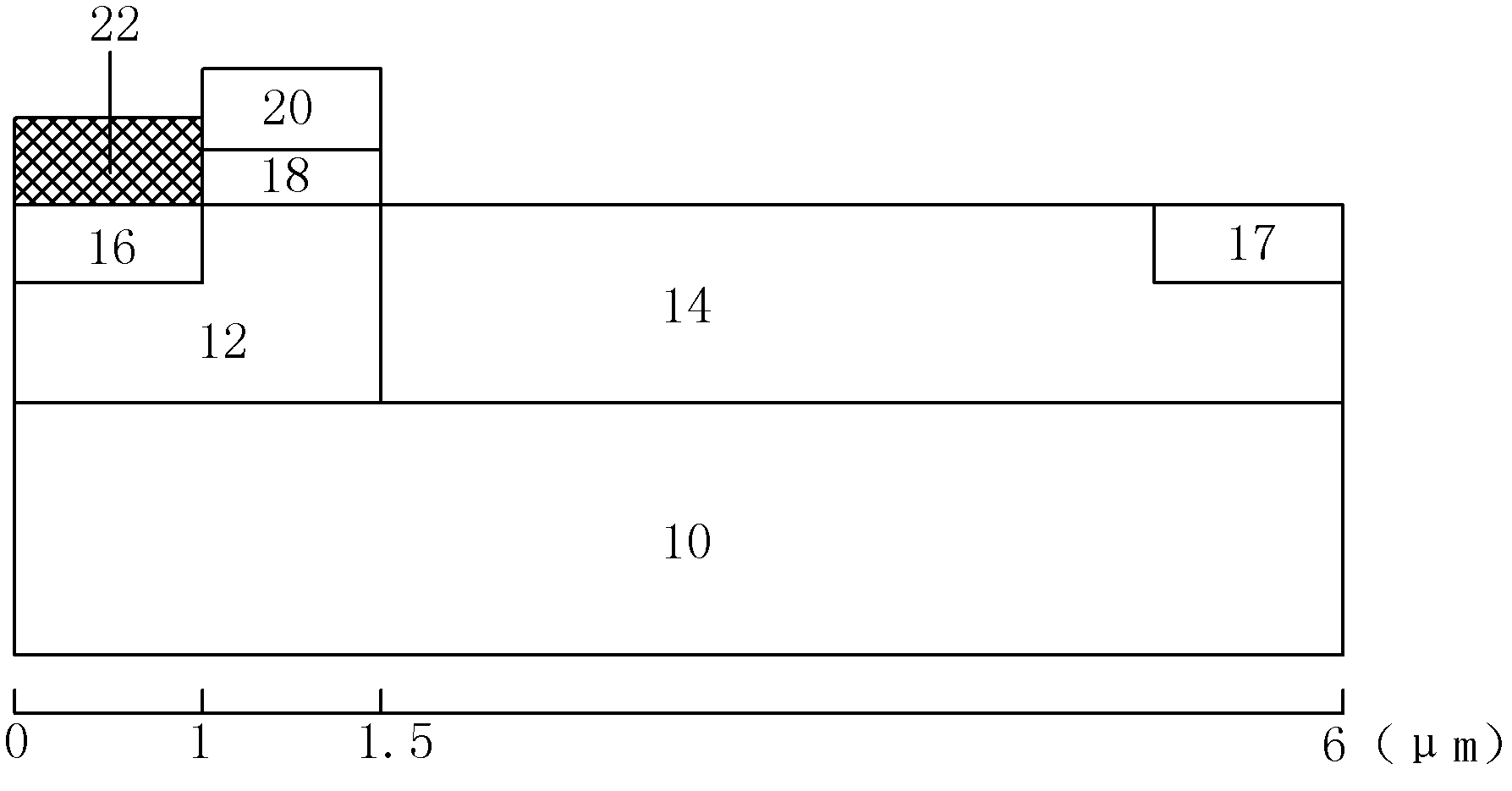
[0032] The cross-sectional structure of the LDMOS device in this example is as follows figure 1 shown. Including a bulk substrate 10, a well region 12 and a drift region 14 adjacent to each other are formed on the substrate 10, a source region 16 and a drain region 17 are respectively formed in the well region 12 and the drift region 14, and a source region 16 and a drain region 14 are formed in the well region 12 and the drift region 14 A gate oxide layer 18 is grown on the surface of the well region 12 between them, and a polysilicon gate 20 is grown on the gate oxide layer 18 . In this example, only the surface of the source region 16 is covered with silicon nitride (Si 3 N 4 ) film 22, using the intrinsic stress of the silicon nitride film 22 to introduce stress into the channel of the LDMOS device. Since the silicon nitride film 22 only exists on the surface of the source region 16 , the stress introduced by it only acts on the nearby channel, and basically does not af...

Embodiment 2

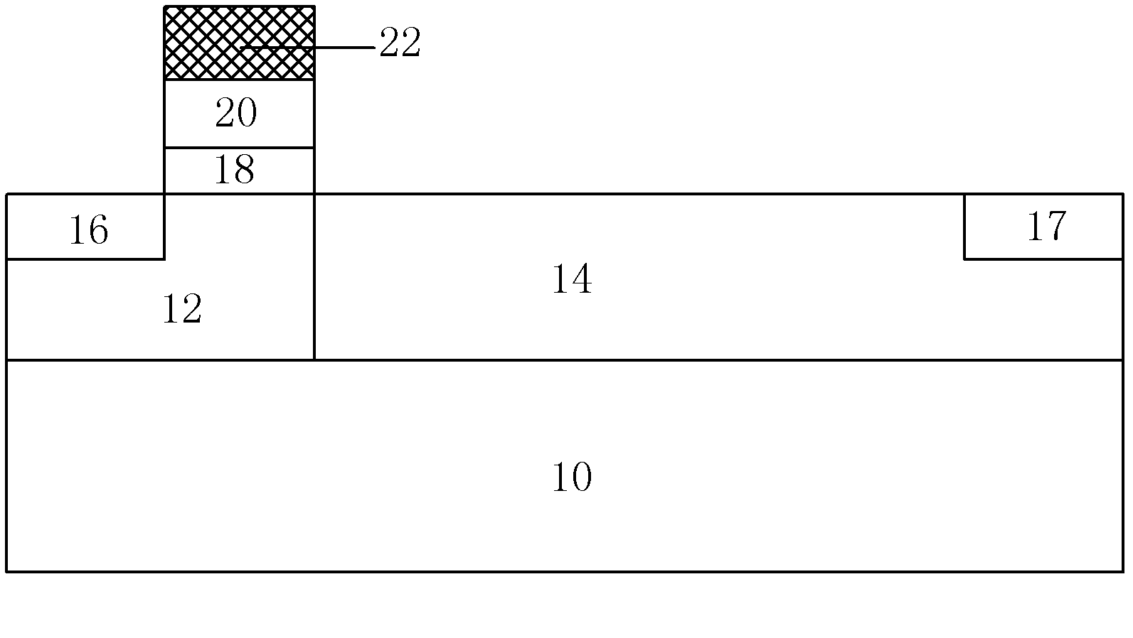
[0034] image 3It is a schematic diagram of the structure of an LDMOS device covered with a silicon nitride film 22 on the surface of the source region 16 and the gate 20 . The manufacturing process of the device of this example is the same as that of Embodiment 1, and the manufacturing of the device body is completed according to the traditional CMOS device manufacturing process, including the preparation of the substrate 10, the formation of the well region 12, the growth of the gate oxide layer 18, the growth of the polysilicon gate 20, the trench ion implantation, drift region 14 ion implantation, source region 16 and drain region 17 ion implantation, and then chemical vapor deposition process is used to deposit nitride with a thickness of 120nm and a tensile stress of 2GPa on the surface of source region 16 and gate 20 Silicon film (22). Next, the fabrication of the entire device is completed through traditional process steps such as local interconnection. The device st...

Embodiment 3

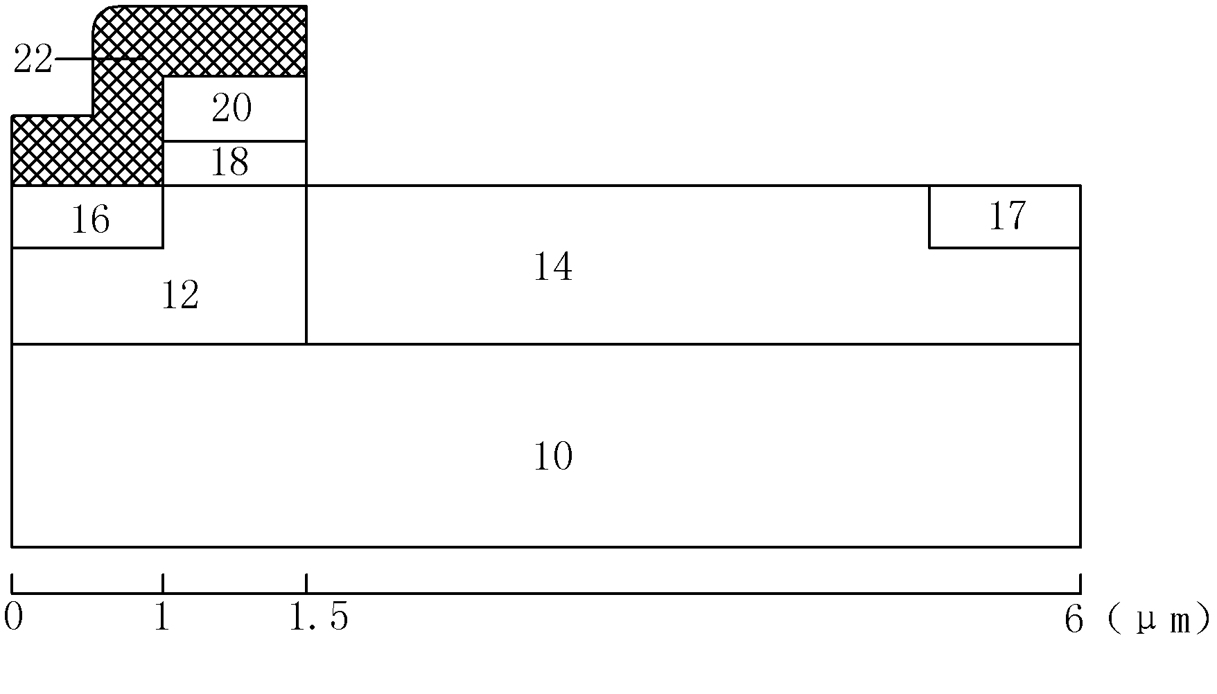
[0036] Figure 4 is a schematic cross-sectional view of the device in this example. The device source region 16 and gate 20 of this example are covered with a silicon nitride film 22, and there is a layer of silicon dioxide (SiO2) between the source region 16 and the silicon nitride film 22. 2 ) film 24. The main function of the silicon dioxide film 24 is to buffer the stress introduced by the silicon nitride covering the surface, so that the stress distribution in the channel region (1-1.5 μm) is relatively uniform. Refer to the description of the above-mentioned embodiment for the manufacturing process of the device body of this example. The manufacturing process of the silicon nitride film 22 of this example is to grow a layer of 20nm thick silicon dioxide film (24) on the surface of the source region 16 first, and then use chemical vapor deposition. A silicon nitride film (22) with a thickness of 120nm and a tensile stress of 2GPa is deposited on the surface of the silic...


PUM

PropertyMeasurementUnit
Thicknessaaaaaaaaaa
Thicknessaaaaaaaaaa

Abstract

The invention relates to a lateral double-diffusion metal oxide semiconductor (LDMOS) device. According to the LDMOS device, the performance is improved by using stress, poor influence is reduced, and the local stress is introduced. The invention adopts the technical scheme that: the LDMOS device introducing the local stress comprises a body substrate, wherein a well area and a drift area, which are adjacent to each other, are formed on the substrate; a source area and a drain area are respectively formed in the well area and the drift area; a gate oxide layer is grown on the surface of the well area between the source area and the drift area; a polycrystalline silicon gate is grown on the gate oxide layer; a thin film covers the surface of the source area and/or the gate; and by using the intrinsic stress of the thin film, the stress is introduced into a channel of the LDMOS device. The LDMOS device has the advantages that: an energy gap (EG) of the drift area of the device cannot be influenced; the on resistance (Ron) of the source area and the drain area of the device can be obviously reduced; a positive effect of the stress on the performance of the device is fully exerted; a negative effect of the stress on the performance of the device is reduced; and the device is particularly applicable to manufacturing of a power device.

Description

technical field [0001] The invention relates to a semiconductor device, in particular to a lateral double-diffused metal oxide semiconductor (LDMOS) device. Background technique [0002] LDMOS device is a semiconductor device developed based on SOI (Semiconductor On Insulator) technology and MOSFET (Metal Oxide Semiconductor Field Effect Transistor) technology, and LDMOS device is usually used as a power device. An ideal power device should have the following ideal static and dynamic characteristics: it can withstand high voltage in the off state; it has a large current and a very low voltage drop in the on state; , Off time, can withstand rapid changes in current and voltage, and has a full control function. The electrodes of the LDMOS device are located on the surface of the chip, and it is easy to realize mutual integration with low-voltage signal circuits and other devices through internal connections. Due to the existence of these advantages, LDMOS devices have been d...

Claims


Application Information

Patent Timeline
IPC IPC(8): H01L29/78H01L29/10
Inventor 王向展郑良晨曾庆平于奇
Owner UNIV OF ELECTRONICS SCI & TECH OF CHINA
Why Eureka
Try Eureka