

Manufacture method of stacked gate SiC-metal insulator semiconductor (MIS) capacitor
A manufacturing method and capacitor technology, applied in the field of microelectronics, can solve problems affecting device mobility, threshold voltage and low-frequency 1/f noise increase, increase leakage current, etc., to improve breakdown characteristics and reliability, reduce Gate leakage current and effect of improving interface characteristics
- Summary
- Abstract
- Description
- Claims
- Application Information
AI Technical Summary
Problems solved by technology
Method used
Image


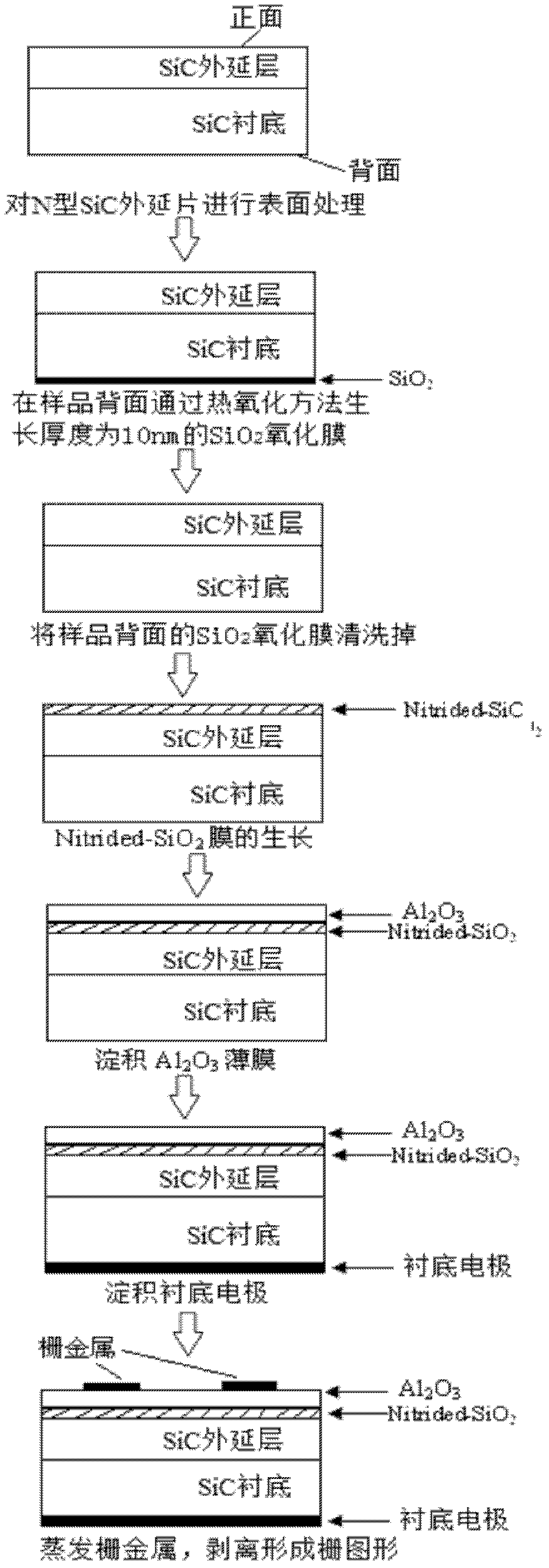
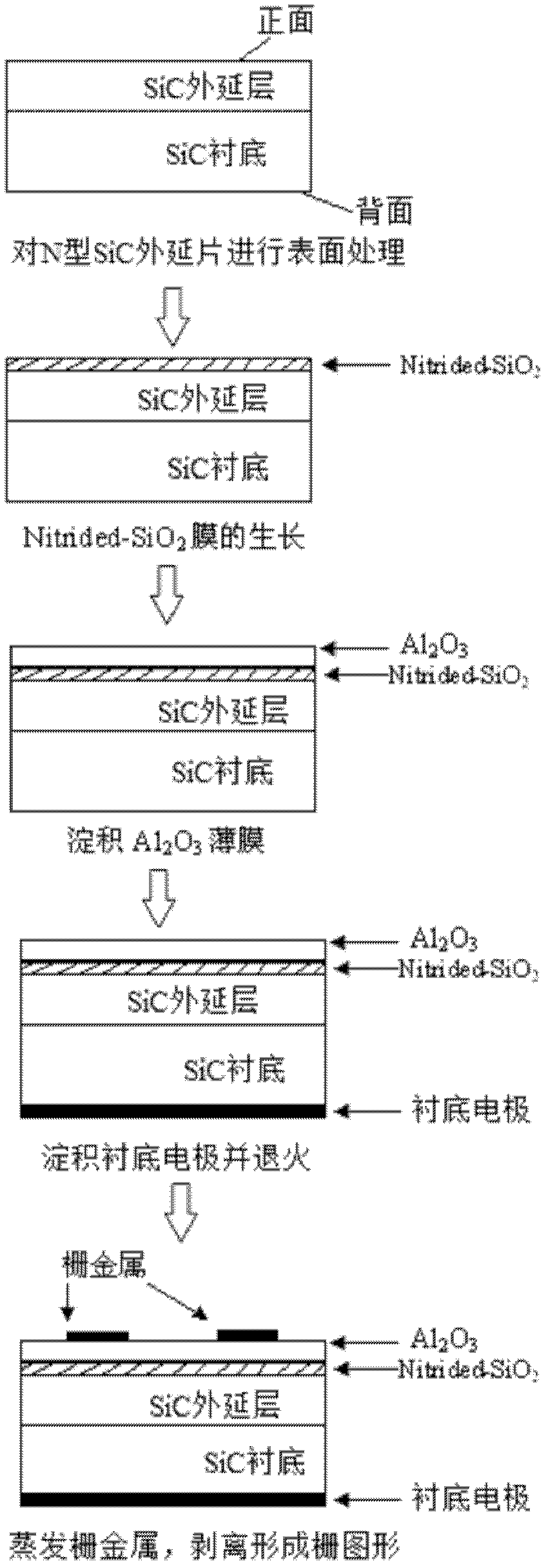
Examples
Embodiment 2
[0079] refer to figure 2 , the implementation steps of this example are as follows:
[0080] Step A, use the standard cleaning method RCA to clean the surface of the 4H-SiC N-type epitaxial wafer sample:
[0081] (A1) Soak the 4H-SiC N-type epitaxial wafer sample in acetone and absolute ethanol for 5 minutes each, and then rinse with deionized water DIW to remove the grease on the surface of the epitaxial wafer sample;
[0082] (A2) Place the SiC sample after the first cleaning in H 2 SO 4 :H 2 o 2 =1:1 solution, soak for 15min, then rinse with deionized water;
[0083] (A3) Place the SiC sample after the second cleaning in HF:H 2 Soak in O=1:10 solution for 1min to rinse off the natural oxide layer, and rinse with deionized water;
[0084] (A4) Immerse the SiC sample after the third cleaning in NH 4 OH:H 2 o 2 : DIW=3:3:10 solution boiled, rinsed with deionized water;
[0085] (A5) Put the SiC sample after the fourth cleaning in HF:H 2 Soak in O=1:10 solution for...
PUM
| Property | Measurement | Unit |
|---|---|---|
| Thickness | aaaaa | aaaaa |
Abstract
Description
Claims
Application Information