Metal substrate vertical GaN-based LED (Light-Emitting Diode) chip and manufacturing method thereof

A technology for LED chips and metal substrates, applied in metal material coating process, gaseous chemical plating, coating, etc., can solve problems such as high deposition temperature, high preparation cost, and difficulty in growing high indium components

Active Publication Date: 2012-10-17
GAOYOU INST CO LTD DALIAN UNIV OF TECH
View PDF4 Cites 14 Cited by
  • Summary
  • Abstract
  • Description
  • Claims
  • Application Information

AI Technical Summary

Problems solved by technology

However, this vertical GaN-based LED manufacturing technology still uses expensive sapphire substrates, and due to the increase of laser lift-off and wafer bonding processes, the process difficulty and manufacturing cost are increased.
[0007] Looking at the existing common MOCVD technolo

Method used


Image

  • Metal substrate vertical GaN-based LED (Light-Emitting Diode) chip and manufacturing method thereof
  • Metal substrate vertical GaN-based LED (Light-Emitting Diode) chip and manufacturing method thereof
  • Metal substrate vertical GaN-based LED (Light-Emitting Diode) chip and manufacturing method thereof

Examples


specific Embodiment approach

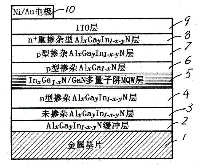
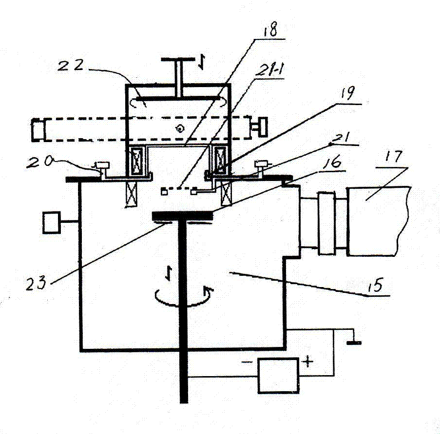
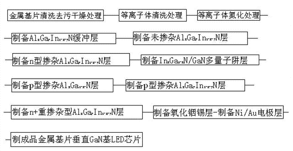
[0073] The second specific implementation mode, as attached figure 1 shown.

[0074] A vertical GaN-based LED chip, including an aluminum substrate (1) with a thickness of 0.5mm, and on one side of the metal aluminum substrate (1), Al x Ga y In 1-x-yN buffer layer (2), undoped Al x Ga y In 1-x-y N layer (3), n-type doped Al x Ga y In 1-x-y N layer (4), In x Ga 1-x N / GaN multiple quantum well MQW layer (5), p-type doped Al x Ga 1-x N layer (6), p-type doped Al x Ga y In 1-x-y N layer(7), n + heavily doped Al x Ga y In 1-x-y N layer (8), indium tin oxide ITO layer (9); Ni / Au electrode layer (10) is arranged on the surface of indium tin oxide ITO layer (9).

[0075] Specific Embodiment 2 The LED chip is prepared using the process steps of Specific Embodiment 1; the chip size is 300 μm×300 μm, when the applied voltage is 3.2V, its luminous wavelength is 515nm, and its brightness is 200mcd. Aluminum substrate vertical GaN-based LED green chip.

[0076] By chang...


PUM


Abstract

The invention discloses a metal substrate vertical GaN-based LED (Light-Emitting Diode) chip and a manufacturing method of the metal substrate vertical GaN-based LED chip. The LED chip is formed by compounding and depositing a metal substrate, an AlxGayIn1-x-yN buffer layer, an undoped AlxGayIn1-x-yN layer, an n-type doped AlxGayIn1-x-yN layer, an InxGa1-xN/GaN multi-quantum well (MQW) layer, a p-type AlxGa1-x-N layer, a p-type doped AlxGayIn1-x-yN layer, an n+ heavy doping type AlxGayIn1-x-yN layer and an indium tin oxide (ITO) layer, wherein an Ni/Au electrode layer is formed on the surface of the ITO layer. The method for manufacturing the metal substrate vertical GaN-based LED chip sequentially comprises the following steps of: arranging materials, performing plasma cleaning, performing nitrogen treatment, manufacturing a buffer layer, manufacturing an undoped layer, manufacturing an n-type doping layer, manufacturing a MQW layer, manufacturing a p-type doping layer, manufacturing a second p-type doping layer, and manufacturing an n+ heavy doping layer, the ITO layer and the electrode layer. The chip has the advantages of reasonable structure, wide spectrum range and the like, and the manufacturing method has the advantages of reasonable process, low temperature, environment friendliness, high quality of finished product, low manufacturing cost and the like.

Description

technical field [0001] The present invention relates to a GaN-based LED chip vertical to a metal substrate and its preparation method, in particular to the Electron Cyclotron Resonance Plasma Enhanced Metalorganic Chemical Vapor Deposition (ECR-PEMOCVD) method. A full-spectrum vertical GaN-based LED chip is prepared on a metal substrate. It belongs to the field of semiconductor light-emitting diode (LED) chip manufacturing. Background technique [0002] Gallium nitride (GaN)-based group III nitride wide bandgap semiconductor materials are the first choice for preparing optoelectronic devices such as light-emitting diodes (LEDs) and semiconductor laser diodes (LDs) in the blue to ultraviolet range. GaN-based materials can obtain a continuously adjustable direct bandgap from 0.7eV (bandgap of indium nitride InN) to 6.2eV (bandgap of aluminum nitride AlN) by adjusting the alloy composition, so that a single system material can be used Optoelectronic devices such as LEDs cover...

Claims


Application Information

Patent Timeline
IPC IPC(8): H01L33/00C23C16/00
Inventor 秦福文林国强刘勤华
Owner GAOYOU INST CO LTD DALIAN UNIV OF TECH
Why Eureka
Try Eureka