Facility for manufacturing vertical GaN-based LED chips by metal substrates

A technology of LED chips and metal substrates, applied in metal material coating process, gaseous chemical plating, coating, etc., can solve the problem of unreasonable layout of gas phase material introduction into reaction chamber, lack of mass flow controller, and improper installation of instruments Reasonable and other issues

Active Publication Date: 2012-10-24
GAOYOU INST CO LTD DALIAN UNIV OF TECH
View PDF7 Cites 21 Cited by
  • Summary
  • Abstract
  • Description
  • Claims
  • Application Information

AI Technical Summary

Problems solved by technology

[0006] Although the above-mentioned existing equipment provides technical equipment support for the preparation of vertical GaN-based LED chips on metal substrates, and has made breakthroughs in low-temperature deposition technology, after all, due to the structural deficiencies in the above-mentioned existing patented technology , such as the unreasonable environment for the deposition of gas phase substances; the unreasonable layout of gas phase substances into the reaction chamber (epitaxy chamber); There are some problems in the coating quality, coating efficiency and preparation cost of the finished vertical GaN-based LED chips.

Method used


Image

  • Facility for manufacturing vertical GaN-based LED chips by metal substrates
  • Facility for manufacturing vertical GaN-based LED chips by metal substrates
  • Facility for manufacturing vertical GaN-based LED chips by metal substrates

Examples


Embodiment Construction

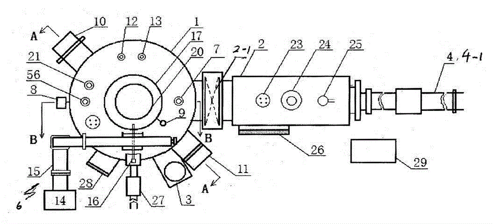
[0039] A typical specific implementation is as attached Figure 1~4 shown.

[0040] A device for preparing vertical GaN-based LED chips using a metal substrate, comprising:

[0041] A computer information acquisition controller 29;

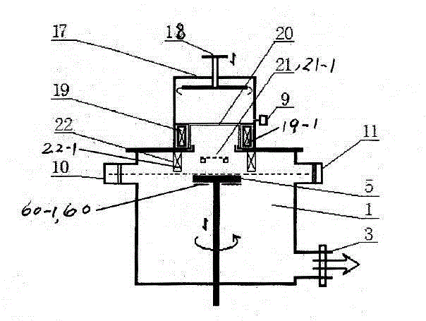
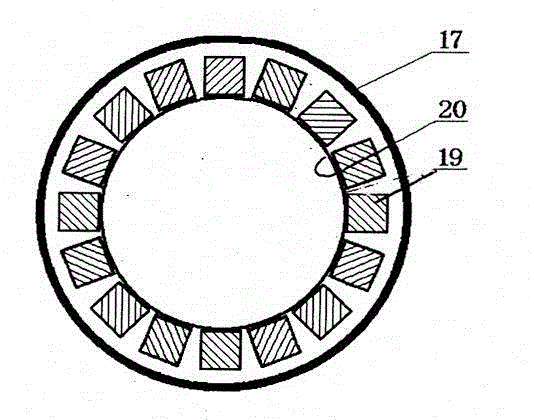
[0042] A reaction chamber 1; in the reaction chamber 1, a mechanical rotary metal substrate table 5 arranged concentrically with the reaction chamber 1 that can move up and down; on the metal substrate table 5, a carbon wire electric heating device 60 is provided; The bottom of the reaction chamber 1 is connected to the pipeline of the vacuum equipment 3, and the negative pressure can be formed in the reaction chamber 1 through the vacuum equipment 3;

[0043] A metal substrate charging chamber 2 including a charging door 26; one end of the metal substrate charging chamber 2 is provided with a magnetic / pneumatic feeding device 4, and the other end is connected to a computer information acquisition controller 29 The electrically connected magnet...


PUM

PropertyMeasurementUnit
heightaaaaaaaaaa

Abstract

The invention discloses a facility for manufacturing vertical GaN-based LED chips by metal substrates. The facility comprises a computer information acquisition controller, a reaction room, a metal substrate feeding room, a gaseous-phase metal organism supply device, a nitrogen and/or hydrogen and/or ammonia supply device, an ECR (electron cyclotron resonance) plasma resource supply device, a vacuum degree meter and an imaging display formed relatively by a reflection high-energy electron diffractometer and a fluorescent screen, and is mainly characterized by further comprising a magnetic field coil support cylinder, a photoelectric alarm, a Faraday cylinder, an electronic probe and a direct-current bias voltage. The facility is reasonable in structure, high in film-coating quality and working efficiency, low in chip manufacture cost and the like.

Description

technical field [0001] The invention relates to a device for preparing a vertical GaN-based LED chip by using a metal substrate, in particular to an electron cyclotron resonance plasma-enhanced metal-organic chemical vapor deposition (ECR-PEMOCVD) device using a cavity-coupled microwave plasma source, belonging to Reactive vapor deposition coating equipment technical field. Background technique [0002] The GaN (gallium nitride)-based LED (light-emitting diode) chip is an LED chip that is coated with a multi-layer GaN-based thin film (nm to μm level) composite coating on the surface of a metal substrate such as aluminum, copper or stainless steel. It can be used to prepare optoelectronic devices such as LEDs covering the spectral range from near-infrared to deep ultraviolet. The full-color display screen made of GaN-based LEDs can be used for multi-color information display in various indoor and outdoor occasions, while white GaN-based LEDs can be used for white lighting an...

Claims


Application Information

Patent Timeline
Patent Type & Authority Applications(China)
IPC IPC(8): H01L33/00H01J37/32C23C16/44C23C16/52
Inventor 秦福文林国强刘勤华
Owner GAOYOU INST CO LTD DALIAN UNIV OF TECH
Why Eureka
Try Eureka