Radio frequency device and manufacturing method thereof

A technology of a radio frequency device and a manufacturing method, applied in the field of microelectronics, can solve the problems of reducing the control ability of the gate to the channel, reducing the concentration of two-dimensional electron gas, and reducing the radio frequency performance of the device, so as to reduce the stress release and improve the radio frequency performance. , the effect of reducing the surface density of states

Active Publication Date: 2012-12-05
DYNAX SEMICON
View PDF5 Cites 18 Cited by
  • Summary
  • Abstract
  • Description
  • Claims
  • Application Information

AI Technical Summary

Problems solved by technology

[0005] However, since the energy band width of aluminum nitride is very wide, exceeding 6 electron volts, it will bring a high Schottky barrier height between the metal and the semiconductor, greatly improving the contact resistance of the source and drain, This in turn degrades the RF performance of the device
In addition, since there is a huge lattice mismatch between AlN and GaN, which will cause stress release in the AlN / GaN heterojunction, additional GaN is required to stabilize the AlN surface. The thickness of the gallium nitride capping layer is usually in the range of 3 to 5 nanometers, which increases the distance between the gate and the two-dimensional electron gas, reduces the control ability of the gate to the channel, and reduces the device's performance. RF performance
Moreover, the Schottky contact of the gate will introduce a large gate leakage current. Usually, people use fluorine treatment to treat the nitride surface with CF4 to form fluoride before depositing the gate metal to reduce the gate leakage current. CF4 treatment will reduce the two-dimensional electron gas concentration in the channel and affect the radio frequency characteristics

Method used


Image

  • Radio frequency device and manufacturing method thereof
  • Radio frequency device and manufacturing method thereof
  • Radio frequency device and manufacturing method thereof

Examples


Embodiment Construction

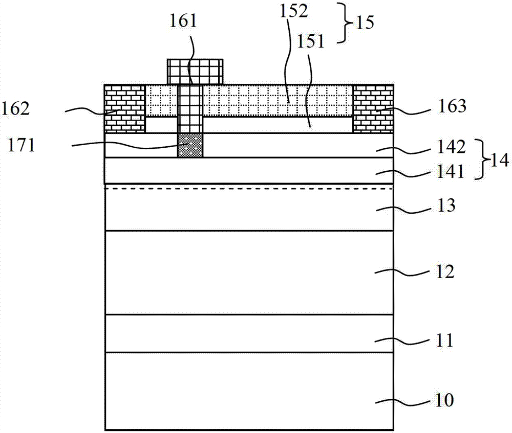
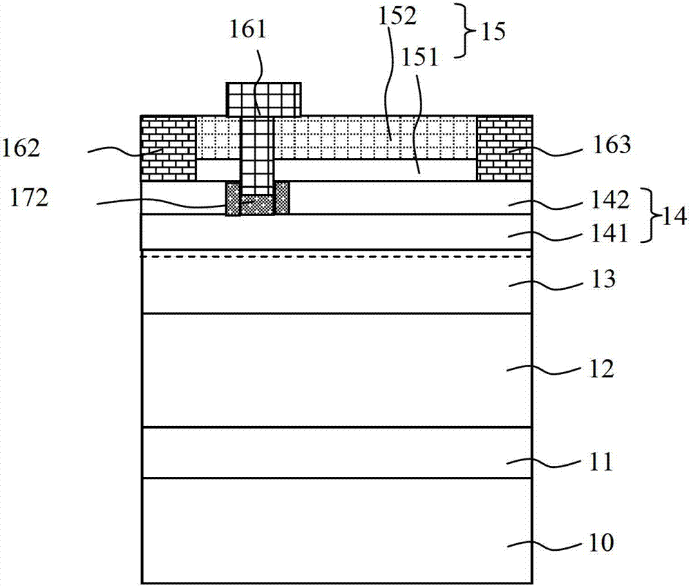
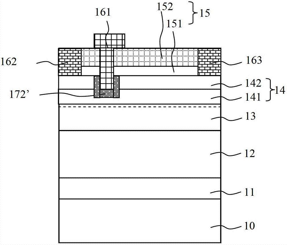
[0050] As mentioned in the background art, the application of aluminum nitride in gallium nitride-based high electron mobility transistors greatly improves the radio frequency performance of the device. However, the wide energy band width makes the aluminum nitride material produce a high Schottky barrier when it is in contact with the metal material, which greatly improves the contact resistance of the drain and source. At the same time, in order to adjust the lattice mismatch between aluminum nitride and gallium nitride, the existing technology often introduces a gallium nitride capping layer on the surface of aluminum nitride, and the gallium nitride capping layer increases the gate to the two-dimensional electron Air distance, thereby degrading the RF performance of the device.

[0051] In order to improve the above two disadvantages and improve the radio frequency performance of GaN-based high electron mobility transistors, the present invention proposes a radio frequency...


PUM

PropertyMeasurementUnit
thicknessaaaaaaaaaa

Abstract

The invention discloses a radio frequency device. A nitride barrier layer of the radio frequency device has two layers of aluminum-rich nitride, wherein aluminum content is more than 75 percent. The second nitride layer is silicon-containing nitride, and silicon content is high enough, so that metal electrodes of drain and source electrodes and the second nitride layer are in ohmic contact, and contact resistance of the drain and source electrodes is reduced; and because the silicon-containing nitride can provide more free electrons, concentration of two-dimensional electron gas is further increased, and radio frequency performance of the device is improved. Meanwhile, a dielectric layer used as a passivation layer of the nitride is grown on the silicon-containing nitride in situ, so that surface state intensity is reduced, and stress releasing is reduced. In the manufacturing process of a grid electrode, the passivation layer of a grid region is etched, and the exposed nitride barrier layer is oxidized. Oxide generated on the grid electrode greatly reduces leakage current of the grid electrode and the leakage current between the source and drain electrodes. In addition, the invention also provides a manufacturing method for the radio frequency device.

Description

technical field [0001] The invention belongs to the technical field of microelectronics, and in particular relates to a radio frequency device and a manufacturing method thereof. Background technique [0002] Gallium nitride, a wide bandgap semiconductor material, is more suitable than silicon and gallium arsenide for making high-temperature, high-frequency, high-voltage and high-power devices. Gallium nitride electronic devices have good application prospects in high-frequency and high-power devices. Since the 1990s, the development of gallium nitride-based radio frequency devices has been one of the hot spots in the research of gallium nitride electronic devices. [0003] The current gain cutoff frequency and the maximum oscillation frequency are two important performance indicators of radio frequency devices. The quality of these two indicators mainly depends on the gate length, the control ability of the gate to the channel, and the contact resistance of the source and ...

Claims


Application Information

Patent Timeline
Patent Type & Authority Applications(China)
IPC IPC(8): H01L29/778H01L29/06H01L21/335
CPCH01L29/7787H01L29/2003H01L29/66462H01L29/42316
Inventor 程凯
Owner DYNAX SEMICON
Why Eureka
Try Eureka